The Graphics Processor
The GeForce GTX 580 graphics processor
So we already stated that for the GeForce GTX 580 NVIDIA went back to the drawing board and introduced a new revision based on the GF100 ASIC, now labeled as the GF110.
With this release, NVIDIA now has a full range of products out on the market from top to bottom. All the new graphics adapters are of course DirectX 11 ready. With Windows 7 and Vista also being DX11 ready all we need are some games to take advantage of DirectCompute, multi-threading, hardware tessellation and new shader 5.0 extensions. DX11 is going to be good and once tessellation kicks into games, much better looking.
- GeForce GTX 580 : 512 SP, 384-bit, 243W TDP
- GeForce GTX 480 : 480 SP, 384-bit, 250W TDP
- GeForce GTX 470 : 448 SP, 320-bit, 225W TDP
The GPU that empowers it all has small architectural changes, some stuff was stripped away and some additional functional units for tessellation, shading and texturing have been added. Make note that the GPU still is big, as the fabrication node is still 40nm. TSMC canceled the 32nm fab node preventing this chip from being smaller.
Both the GF100 and GF110 graphics processors have sixteen shader clusters embedded in them (called SMs). For the GeForce GTX 480 one such a cluster was disabled and on the GeForce GTX 470 two were actually disabled. The GTX 580 has the full 512 shader processors activated, meaning a notch more performance just based on that alone already. So that's 512 shader processors, 32 more than the GTX 480 had.
Finally, to find some additional performance, the card got clocked a chunk faster at 772 MHz as well, whereas the GeForce GTX 480 was clocked at 700 MHz.
| GeForce 9800 GTX |
GeForce GTX 285 |
GeForce GTX 295 |
GeForce GTX 470 |
GeForce GTX 480 |
GeForce GTX 580 | |
| Stream (Shader) Processors | 128 | 240 | 240 x2 | 448 | 480 | 512 |
| Core Clock (MHz) | 675 | 648 | 576 | 607 | 700 | 772 |
| Shader Clock (MHz) | 1675 | 1476 | 1242 | 1215 | 1400 | 1544 |
| Memory Clock (effective MHz) | 2200 | 2400 | 2000 | 3350 | 3700 | 4000 |
| Memory amount | 512 MB | 1024 MB | 1792 MB | 1280 | 1536 | 1536 |
| Memory Interface | 256-bit | 512-bit | 448-bit x2 | 320-bit | 384-bit | 384-bit |
| Memory Type | gDDR2 | gDDR3 | gDDR3 | gDDR5 | gDDR5 | gDDR5 |
| HDCP | Yes | Yes | Yes | Yes | Yes | Yes |
| Two Dual link DVI | Yes | Yes | Yes | Yes | Yes | Yes |
| HDMI | No | No | No | Yes | Yes | Yes |
For Fermi NVIDIA made their memory controllers GDDR5 compatible, which was not the case on GT200 based GeForce GTX 260/275/285/295, hence their GDDR3 memory.
Memory wise NVIDIA has large expensive memory volumes due to their architecture, we pass 1 GB as standard these days for most of NVIDIA's series 400 and 500 graphics cards. Each memory partition utilizes one memory controller on the respective GPU, which will get 256MB of memory tied to it.
- The GTX 470 has five memory controllers (5x256MB) = 1280 MB of GDDR5 memory
- The GTX 480 has six memory controllers (6x256MB) = 1536 MB of GDDR5 memory
- The GTX 580 has six memory controllers (6x256MB) = 1536 MB of GDDR5 memory
As you can understand, the massive memory partitions, bus-width and combination of GDDR5 memory (quad data rate) allow the GPU to work with a very high framebuffer bandwidth (effective). Let's put most of the data in a chart to get an idea and overview of changes:
| Graphics card | GeForce GTX 470 | GeForce GTX 480 | GeForce GTX 580 |
| Fabrication node | 40nm | 40nm | 40nm |
| Shader processors | 448 | 480 | 512 |
| Streaming Multiprocessors (SM) | 14 | 15 | 16 |
| Texture Units | 56 | 60 | 64 |
| ROP units | 40 | 48 | 48 |
| Graphics Clock (Core) | 607 MHz | 700 MHz | 772 MHz |
| Shader Processor Clock | 1215 MHz | 1401 MHz | 1544 MHz |
| Memory Clock / Data rate | 837 MHz / 3348 MHz | 924 MHz / 3696 MHz | 1000 MHz / 4000 MHz |
| Graphics memory | 1280 MB | 1536 MB | 1536W MB |
| Memory interface | 320-bit | 384-bit | 384-bit |
| Memory bandwidth | 134 GB/s | 177 GB/s | 192 GB/s |
| Power connectors | 2x6-pin PEG | 1x6-pin PEG, 1x8-pin PEG | 1x6-pin PEG, 1x8-pin PEG |
| Max board power (TDP) | 215 Watts | 250 Watts | 244 Watts |
| Recommended Power supply | 550 Watts | 600 Watts | 600 Watts |
| GPU Thermal Threshold | 105 degrees C | 105 degrees C | 97 degrees C |
So we talked about the core clocks, specifications and memory partitions. Obviously there's a lot more to talk through. Now, at the end of the pipeline we run into the ROP (Raster Operation) engine and the GTX 580 again has 48 units for features like pixel blending and AA.
There's a total of 64 texture filtering units available for the GeForce GTX 580. The math is simple here, each SM has four texture units tied to it.
- GeForce GTX 470 has 14 SMs X 4 Texture units = 56
- GeForce GTX 480 has 15 SMs X 4 Texture units = 60
- GeForce GTX 580 has 16 SMs X 4 Texture units = 64
Though still a 40nm based chip, the GF110 GPU comes with almost 3 billion transistors embedded into it. The TDP remains the same at roughly 240~250 Watts, while performance goes up ~20%.
TDP = Thermal Design Power. Roughly translated, when you stress everything on the graphics card 100%, your maximum power consumption is the TDP.
The GeForce GTX 580 comes with both a 6-pin and 8-pin power connector to get enough current and a little spare for overclocking. This boils down as: 8-pin PEG = 150W + 6-pin PEG = 75W + PCIe slot = 75W is 300W available (in theory).
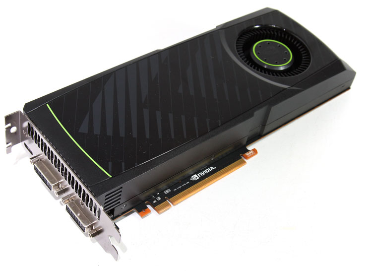 Geforce GTX 580 reference graphics card, powered by the GF110 GPU
