
Pascal GPU Architecture
The Pascal GP107 GPU
The GPU is based on a DX12 compatible architecture called Pascal. Much like in the past designs you will see pre-modeled SMX clusters that hold what is 2x64 shader processors per cluster. Pascal GPUs are composed of different configurations of Graphics Processing Clusters (GPCs), Streaming Multiprocessors (SMs), and memory controllers. Each SM is paired with a PolyMorph Engine that handles vertex fetch, tessellation, viewport transformation, vertex attribute setup, and perspective correction. The GP107 PolyMorph Engine also includes new Simultaneous Multi-Projection units. There are 6 active (SM) clusters for a fully enabled Pascal GP107 GPU. The GeForce GTX 1050 Ti is fully enabled, the non-Ti model 1050 thus has one cut out thus holding 5 SM clusters.
- The GeForce GTX 1050 (GP107-300) has 5 x 128 shader processors which make a total of 640 shader processors.
- The GeForce GTX 1050 3GB (GP107-301) has 6 x 128 shader processors which make a total of 768 shader processors.
- The GeForce GTX 1050Ti (GP107-400) has 6 x 128 shader processors which make a total of 768 shader processors.
- The GeForce GTX 1060 (3GB) (GP104-400) has 9 x 128 shader processors which make a total of 1,152 shader processors.
- The GeForce GTX 1060 (6GB) (GP104-400) has 10 x 128 shader processors which make a total of 1,280 shader processors.
- The GeForce GTX 1070 (GP104-200) has 15 x 128 shader processors which make a total of 1,920 shader processors.
- The GeForce GTX 1080 (GP104-400) has 20 x 128 shader processors which make a total of 2,560 shader processors.
Each SM, however, has a cluster of 64 shader / stream / cuda processors doubled up. Don't let that confuse you, it is 128 shader units per SM. Each GPC ships with a dedicated raster engine and five SMs. Each SM contains 128 CUDA cores, 256 KB of register file capacity, a 96 KB shared memory unit, 48 KB of total L1 cache storage, and eight texture units. As far as the memory specs of the GP107 GPU are concerned, these boards will feature a 96 or 128-bit memory bus connected to 2,3 or 4 GB of GDDR5 video memory, AKA VRAM AKA framebuffer AKA graphics memory for the graphics card. The GeForce GTX 1000 series are DirectX 12 ready, in our testing, we'll address some Async compute tests as well. The latest revision of DX12 is a Windows 10 feature only but can bring in significant optimizations. For your reference, below is a quick overview of some past generation high-end GeForce cards. With 4 GB graphics memory available for one GPU, the GTX 1050 Ti is very attractive for entry level modern and future games no matter what resolution you game at. 1080P and 4 GB are fine.
Pascal Graphics Architecture
Let's place the more important data on the GPU into a chart to get an idea and better overview of changes in terms of architecture like shaders, ROPs and where we are at frequencies wise:
 | ||||||
|---|---|---|---|---|---|---|
| GeForce | Titan X | GTX 1080 | GTX 1070 | GTX 1060 | GTX 1050 Ti | GTX 1050 |
| (2016 edition) | ||||||
| GPU | GP102-400-A1 | GP104-400-A1 | GP104-200-A1 | GP106-400-A1 | GP107-400-A1 | GP107-30x-A1 |
| Architecture | Pascal | Pascal | Pascal | Pascal | Pascal | Pascal |
| Transistor count | 12 Billion | 7.2 Billion | 7.2 Billion | 4.4 Billion | 3.3 Billion | 3.3 Billion |
| Fabrication Node | 16 nm | 16 nm | 16 nm | 16 nm | 14 nm | 14 nm |
| CUDA Cores | 3,584 | 2,560 | 1,920 | 1,280 | 768 | 768/640 |
| SMMs / SMXs | 28 | 20 | 15 | 10 | 6 | 6/5 |
| ROPs | 96 | 64 | 64 | 48 | 32 | 24/32 |
| GPU Clock Core | 1,417 MHz | 1,607 MHz | 1,506 MHz | 1,506 MHz | 1,290 | 1,354 MHz |
| GPU Boost clock | 1,531 MHz | 1,733 MHz | 1,683 MHz | 1,709 MHz | 1,392 | 1,455 MHz |
| Memory Clock | 2500 MHz | 1,250 MHz | 2,000 MHz | 2,000 MHz | 1,752 MHz | 1,752 MHz |
| Memory Size | 12 GB | 8 GB | 8 GB | 6 GB | 4 GB | 3/2 GB |
| Memory Bus | 384-bit | 256-bit | 256-bit | 192-bit | 128-bit | 96/128-bit |
| Memory Bandwidth | 480 GB/s | 320 GB/s | 256 GB/s | 192 GB/s | 112 GB/s | 84/112 GB/s |
| FP Performance | 11.0 TFLOPS | 9.0 TFLOPS | 6.45 TFLOPS | 4.61 TFLOPS | 2.2 TFLOPS | 1.9 TFLOPS |
| GPU Thermal Threshold | 94 Degrees C | 94 Degrees C | 94 Degrees C | 94 Degrees C | 97 Degrees C | 97 Degrees C |
| TDP | 250 Watts | 180 Watts | 150 Watts | 120 Watts | 75 Watts | 75 Watts |
| Launch MSRP ref | $1200 | $599/$699 | $379/$449 | $249/$299 | $139 | $109 |
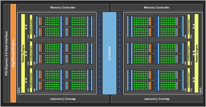
So we talked about the core clocks, specifications, and memory partitions. However, to be able to better understand a graphics processor you simply need to break it down into tiny pieces. Let's first look at the raw data that most of you can understand and grasp. This bit will be about the architecture. NVIDIA’s “Pascal” GPU architecture implements a number of architectural enhancements designed to extract even more performance and more power efficiency per watt consumed. Above, in the chart photo, we see the block diagram that visualizes the architecture, Nvidia started developing the Pascal architecture around 2013/2014 already. The GPCs has 6 SMX/SMM (streaming multi-processors) clusters in total. You'll spot six 32-bit memory interfaces, bringing in a 128-bit path to the graphics GDDR5 or GDDR5X memory. Tied to each 32-bit memory controller are eight ROP units and 256 KB of L2 cache. The full GP107 chip used in the GTX 1050 Ti thus has a total of 32 ROPs and 1,024 KB of L2 cache.
A fully enabled GP104 GPU will have (GTX 1080):
- 2,560 CUDA/Shader/Stream processors
- There are 128 CUDA cores (shader processors) per cluster (SM)
- 7.1 Billion Transistors (FinFet at 16 nm)
- 160 Texture units
- 64 ROP units
- 2 MB L2 cache
- 256-bit GDDR5X
A partially disabled GP104 GPU will have (GTX 1070):
- 1,920 CUDA/Shader/Stream processors
- There are 128 CUDA cores (shader processors) per cluster (SM)
- 7.1 Billion Transistors (FinFet at 16 nm)
- 120 Texture units
- 64 ROP units
- 2 MB L2 cache
- 256-bit GDDR5
A fully enabled GP106 GPU will have (GTX 1060):
- 1,280 CUDA/Shader/Stream processors
- There are 128 CUDA cores (shader processors) per cluster (SM)
- 4 Billion Transistors (FinFet at 16 nm)
- 80 Texture units
- 48 ROP units
- 2 MB L2 cache
- 192-bit GDDR5
A fully enabled GP107 GPU will have (GTX 1050 (Ti)):
- 768 CUDA/Shader/Stream processors
- There are 128 CUDA cores (shader processors) per cluster (SM)
- 3.3 Billion Transistors (FinFet at 16 nm)
- 48 Texture units
- 32 ROP units
- 1 MB L2 cache
- 128-bit GDDR5
- GeForce GTX 960 has 8 SMX x 8 Texture units = 64
- GeForce GTX 970 has 13 SMX x 8 Texture units = 104
- GeForce GTX 980 has 16 SMX x 8 Texture units = 128
- GeForce GTX Titan X has 24 SMX x 8 Texture units = 192
- GeForce GTX 1050 (2GB) has 5 SMX x 8 Texture units = 40
- GeForce GTX 1050 (3GB) has 6 SMX x 8 Texture units = 48
- GeForce GTX 1050 Ti (4GB) has 6 SMX x 8 Texture units = 48
- GeForce GTX 1060 (3GB) has 9 SMX x 8 Texture units = 72
- GeForce GTX 1060 (6GB) has 10 SMX x 8 Texture units = 80
- GeForce GTX 1070 has 15 SMX x 8 Texture units = 120
- GeForce GTX 1080 has 20 SMX x 8 Texture units = 160
So there's a total of 6 SMX x 8 TU = 48 texture filtering units available (Ti).
