Product Innards
Product Innards
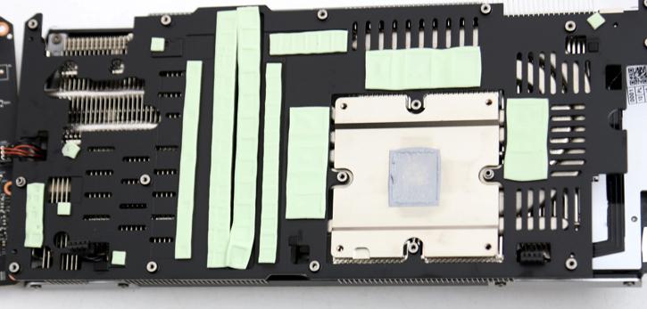
The cooling solution is easy to remove. You will spot an aluminum heatsink tied to the GPU base block. Thermal paste applied to the GPU, all VRM and DDR5X memory has been thermally cushioned. So not just the GPU but also VRAM and MOSFETs are cooled. The also has been done on the backside as you can see the cushioning in the back-plates.
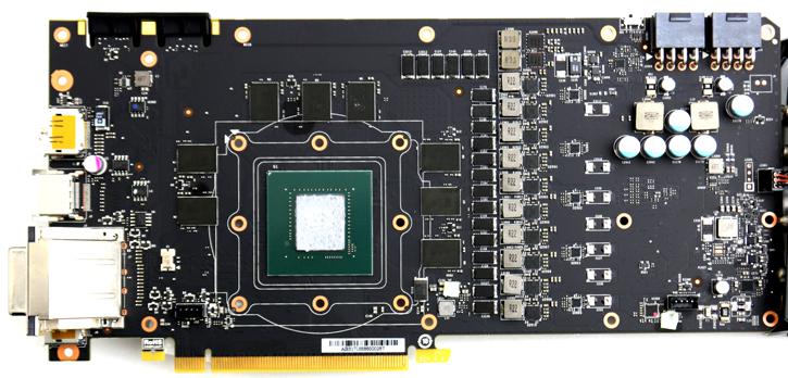
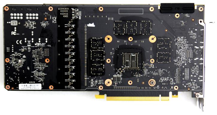
With the main cooler is removed, you can see the PCB and its components. Overall a very clean looking PCB, with a rather impressive looking power design.
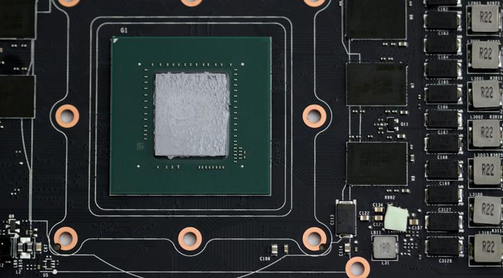
Here we have the GP104-400-A1 graphics processor from Nvidia surrounded by the GDDR5X memory chips.
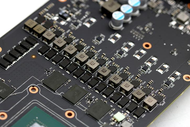
The board has power 12-phases, you will spot proper grade chokes and capacitors. The idea is that the 10 (gpu) +2 (mem) power phases on the card make the MOSFET working at a lower temperature and (should) provide more stable voltage output. This kind of heat protection and load balance to each MOSFET can effectively extend the card's life.
If we zoom in a little we think we spot a uP9511 controller, this is voltage controller for NVIDIA cards in the 1080 range. The unit however is listed as 8 Phase Buck controller. If this is correct then EVGA is likely doubling up the phases to get to 2x5 + 2 of them. It is difficult to read though, so I cannot draw any conclusions from this just yet.
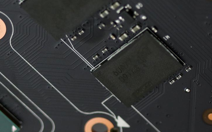
The card makes use of Micron GDDR5X memory ICs, these are rated 10 Gbps and tweaked you surely will get close to a range of 11 Gbps.
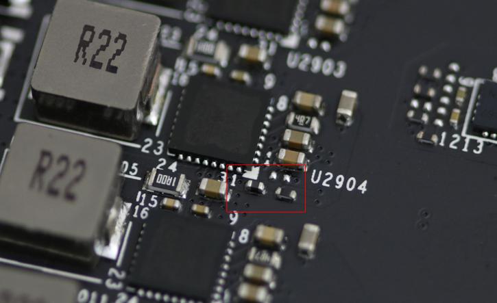
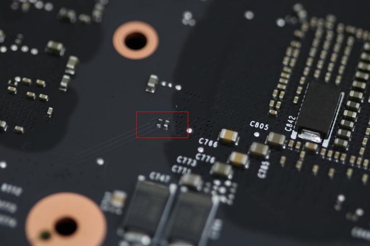
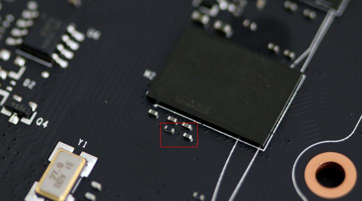
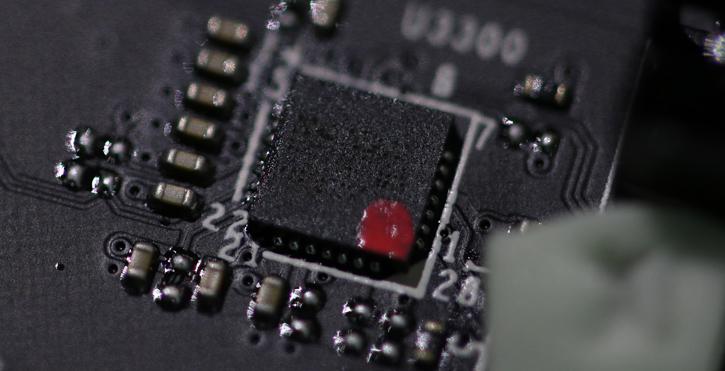
So what am I highlighting here in red? Well these would be the thermal sensors, nine of them have been placed throughout the PCB on both the front and backside. I had to use a macro lens here, as gosh these critters are small.
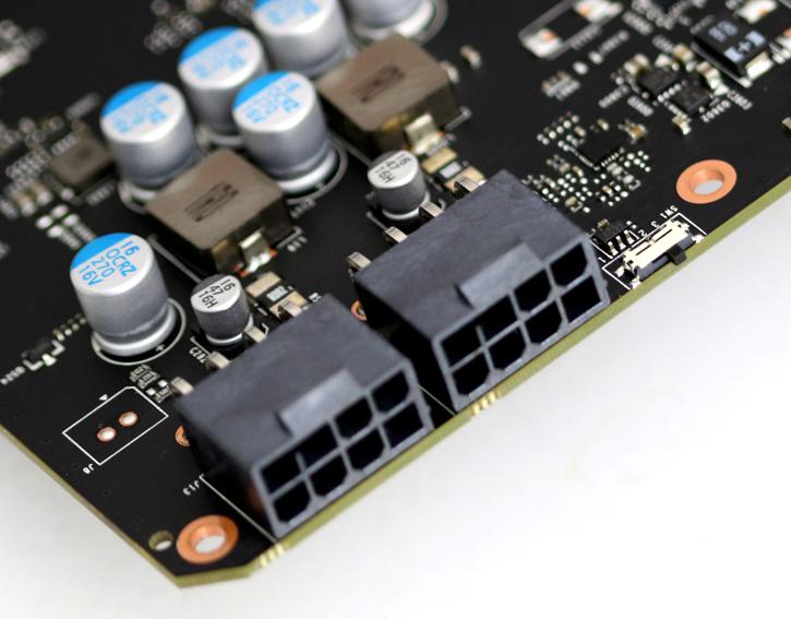
Last but not least, to the right of the two 8-pin PCIe power headers you can see one micro-switch, should you mess up your firmware, shift it into position one and you'll have the card up and running again thanks to a secondary BIOS.
