Page 2
The Building
ECS HQ is based in the financial district of Taipei, Taiwan. The 97 meters high building houses roughly 500-600 employees from all segments like marketing, sales, accounting, research and development, management but also the simple stuff cafeteria. I think two meals a day are served in the cafeteria each day that all ECS employees can use, as small portion of their wages go to this food service.
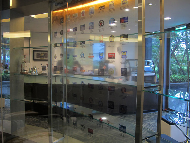
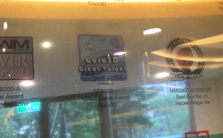
Below some photo's of the buildings entry hall, covering a nice large board with awards they received and yes Guru3D.com is on the board, at least four times based on a quick count.
You'll notice some photo's on reception area, conference halls and cafeteria.
So how does ECS create its hardware ? Well now we get to the good stuff. Hardware research and development. ECS follows a stringent design processes, the major design steps go as follows:
- Project start / cost orientation - in this first step product positioning, pricing and channel related information is discussed, e.g. what features does the product have versus cost and profits.
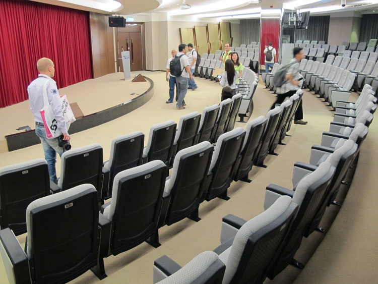 One of the ECS meeting and conference rooms
