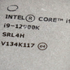
12th Generation Core series processors
Alder Lake - Hybrid Computing Architecture
It hasn't exactly been a secret that Intel has been putting in significant effort to re-take the CPU market. After numerous respins, it was time for a new architecture, created from the ground up with a hybrid design; meet Alder Lake, which you've probably already heard a lot about. These processors will be the first to adopt a hybrid architecture, similar to ARM's BIG.little, that combines high-performance cores combined with efficient ones, making them the first of their kind for Intel. Furthermore, this new generation is now proven to be the first to support DDR5 memory (DDR4 compatible memory controllers as well) and PCI-Express 5.0, making it the first generation to do so. Mind you the Core i9-12900K has 16 cores and 24 threads. 8 P-Core (16 threads) and 8 E-Core (with 8 threads). The CPU has 30 MB L3 cache, 3 MB per core (Golden Cove), and 3 MB per cluster (E-Core) (Gracemont). That's 8 P-Cores for 24 MB and 6 MB from each of the two clusters of 4 E-Cores. The chip has 12.5 MB of L2 cache and 1.25 MB of L3 cache.
- L2 cache 10MB (8x 1.25MB) + 2MB (8x 256kB)
- L3 cache 30MB
| Rocket Lake-S | Alder Lake-S | Raptor Lake-S | Meteor Lake-S | Lunar Lake-S | |
|---|---|---|---|---|---|
| Launch Date | March 30, 2021 | Q4 2021 | Q4 2022 | 2023 (?) | 2024 (?) |
| Fabrication Node | 14nm | Intel 7 | Intel 7 | Intel 4 | TBC |
| Core µArch | Cypress Cove | Golden Cove + Gracemont | Raptor Cove + Gracemont | Redwood Cove + Gracemont (?) | TBC |
| Graphics µArch | Gen12.1 | Gen12.2 | Gen12.2 | Gen 12.7 | Gen 13 |
| Max Core Count | up to 8 cores | up to 16 (8C+8c) | up to 24 (8C+16c) | TBC | TBC |
| Socket | LGA1200 | LGA1700 | LGA1700 | TBC | TBC |
| Memory Support | DDR4 | DDR4/DDR5 | DDR5 | DDR5 | DDR5 |
| PCIe Gen | PCIe 4.0 | PCIe 5.0 | PCIe 5.0 | PCIe 5.0 | PCIe 5.0 |
| Intel Core Series | 11th Gen Core-S | 12th Gen Core-S | 13th Gen Core-S | 14th Gen Core-S | 14th Gen Core-S |
| Motherboard Chipsets | Intel 500 (Z590) | Intel 600 (eg. Z690) | Intel 700 (Z790) | - | - |
Gracemont (energy-efficient cores)
Alder Lake is Intel's codename for the 12th-generation of Intel Core processors based on a hybrid architecture utilizing Golden Cove high-performance cores and Gracemont power-efficient cores. According to Intel, Alder Lake is a "performance hybrid" in their portfolio, as it is focused on performance rather than power consumption. Gracement, wasn't that Intel Atom related? Gracemont is an upcoming microarchitecture for low-power processors that will also be used in Intel's systems on a chip (SoCs). It will be the successor of the Tremont microarchitecture. Additionally, it will be deployed as low-power cores in a hybrid architecture for Intel's Alder Lake processors, similar to its predecessor. The cores have been further enhanced. Gracemont is actually the 4th generation out-of-order low-power Atom microarchitecture, built on the Intel 7 manufacturing process. Intel also says that Alder Lake will provide the most performance per watt of any of its processors. You're going to notice a number of things, among them, increases in L1 caches; the Instructions cache for example was doubled to 64KB with an up to 4MB L2 cache, remember we're still talking the energy-friendly cores here. Microsoft will have to introduce support for these sophisticated scheduling features to x86-64 Windows in order for them to be supported for the next-generation hardware schedulers. Key changes:
- 64KB per core Level 1 instruction cache
- DDR5 memory
- PCIe 5.0 support
- Support for AVX, AVX2, and AVX-VNNI instructions
Golden Cove (performance cores)
Alder Lake will also make use of its Golden Cove CPU cores when speed and performance are critical. And these should make a significant difference in IPC when it comes to processing data compared to say Comet- and Rocket lake. Golden Cove CPU microarchitecture will take the place of the Sunny Cove, Willow Cove, and Cypress Cove microarchitectures, according to Intel. Originally described to as 10 nm Enhanced SuperFin, it will be made using Intel's Intel 7 manufacturing node, which was introduced in 2012. (10ESF). These high-performance cores will find their way into scalable processors such as Alder Lake and Xeon, as well as Sapphire Rapids. According to Intel, all of the enhancements combined should result in an improvement in IPC of 19 percent, which is on par with or slightly higher than the improvement achieved by Sunny Cove when compared to Skylake. That should even be sufficient to dethrone the Zen 3 architecture of the Ryzen 5000 CPUs.
| Product code | Core | Thread | Clock speed | L3 cache | |||||
| Base clock E |
Boost Clock E |
Base Clock P |
Boost Clock P All cores |
Boost Clock P 1-core |
|||||
| Core i9-12900K | BX8071512900K | 8P+8E | 24 | 2.4 | 3.9 | 3.2GHz | 5.2 | 5.3GHz | 30MB |
| Core i9-12900KF | BX8071512900KF | 8P+8E | 24 | 2.4 | 3.9 | 3.2GHz | 5.2 | 5.3GHz | 30MB |
| Core i7-12700K | BX8071512700K | 8P+4E | 20 | 2.7 | 3.8 | 3.6GHz | 5.0 | 5.0GHz | 25MB |
| Core i7-12700KF | BX8071512700KF | 8P+4E | 20 | 2.7 | 3.8 | 3.6GHz | 5.0 | 5.0GHz | 25MB |
| Core i5-12600K | BX8071512600K | 6P+4E | 16 | 2.8 | 3.6 | 3.7GHz | - | 4.9GHz | 20MB |
| Core i5-12600KF | BX8071512600KF | 6P+4E | 16 | 2.8 | 3.6 | 3.7GHz | - | 4.9GHz | 20MB |
So there you have it. Alder Lake-S will include 8 Golden Cove cores and 8 Gracemont cores, according to Intel, who verified this during the company's architecture day. It will be manufactured utilizing Intel's Intel 7 technology, which was previously known as the Intel 10 nm Enhanced SuperFin process. As previously stated, Alder Lake-S will have 8 Golden Cove cores, which are high-performance cores, and 8 Gracemont cores, which are high-efficiency cores. Due to the fact that Gracemont cores do not support Hyper-Threading (HT), Alder Lake-S will only be able to provide 16 cores and 24 threads, which is the same as the i9-12900K configuration.
CPU
- Further information: Golden Cove (microarchitecture) and Gracemont (microarchitecture)
- Golden Cove high-performance CPU cores
- New instruction set extensions[6]
- Gracemont high-efficiency CPU cores
- Next-generation hardware scheduler; adding support for these advanced scheduling capabilities will require Microsoft to add support for them to x86-64 Windows.
GPU
- Intel Xe (Gen12.2) GPU
I/O
- New LGA 1700 socket[8]
- PCI Express 5.0
- DDR5 memory support for desktop CPUs
- LPDDR5 memory support for laptop CPUs
- DMI 4.0 x8 link with Intel 600 series PCH chipsets
Above you can see three markets differentiated versions of Alder lake. For us, Guru's the most left one is the most important. It is possible to view the eight high-performance cores (golden cove) in dark blue, as well as the energy-efficient Gracemont cores, which are visible below them in light blue. The integrated graphics is based on Xe, and it has up to 96 EUs for the GPU and 32 EUs for media functionality only, according to the manufacturer. For a fully equipped processor, you'll receive eight performance cores as well as eight energy-efficient cores; the performance cores have SMT (hyper-threading), which means you'll end up with a total of 24 CPU threads. In the following chapters, we'll dive into greater depth about architecture. The initial release of alder lake will see 3 primary SKUs.
DDR5 Memory subsystem
Following the release of Intel's new generation of desktop processors, it is now the turn of the memory to catch up with the processor. Alder Lake not only supports the well-known ddr4 memory standard, but it also supports the more recent DDR5 memory standard. Several firms have already demonstrated their DIMMs often with transfer rates as high as 8,400 MT/s per second, in addition to the conventional ddr5-4800 modules with case latency 40 and capacities as high as 8, 16, and 32GB per DIMM. There is support for on-die error correction code, as well as XMP Profile 3.0, which makes overclocking more straightforward. Using the new generation, the power feed has been relocated from the motherboard to the power management integrated circuit, also known as the pmic, which is located on the module itself. Intel continues to list memory at the JEDEC specification level, implying that it is unable to go any further. DDR4 memory operates at 3200 MHz, while DDR5 memory operates at 4800 MHz by default. You can already see that the memory bandwidth is likely to rise dramatically with DDR5 technology. So support at JEDEC defaults is Dual Channel PC5-38400U (DDR5-4800) or PC4-25600U (DDR4-3200).
New and included in DDR5 is XMP 3.0, in total 5, but up to three manufacturer timing and frequency profiles can now be stored inside the DIMM. However, 2 remaining profiles can be configured and written by the end-user. meaning if you can find a sweet spot for your memory (frequency, timings, and voltage wise) you can store that profile to SPD.
PCI Express 5.0
Alder Lake will enable PCI Express 5.0, which will more than double the bandwidth available from Gen 4, reaching a whopping 64 GB/s over 16 lanes, as predicted by rumors and now confirmed by Intel. Comparatively, PCIe Gen 3.0 (which is fast) can carry 16 GB/s across 16 lanes. Interconnects will be required to connect everything together. AMD refers to this as the infinity fabric, whereas Intel refers to it as the compute fabric; two distinct names for the same concept. The DMI interface between CPU and chipset also has received a massive upgrade to DMI 4.0, 16GT/s (PCIe 4.0 x8).
The Z690 chipset
Intriguing is the diagram for the Z690 chipset, which is the highest-end model released first. The CPU has 16 (or 2 times 8 PCIe 5.0 lanes), which can be used for graphics or storage, in addition to four NVME 4.0 lanes. What was previously said appears to be correct; the chipset has 12 times gen4 and 16 times gen3 processors. Additional features include support for two DIMMs per memory channel and dual-channel DDR4-3200 or DDR5-4800 with two DIMMs per memory channel.
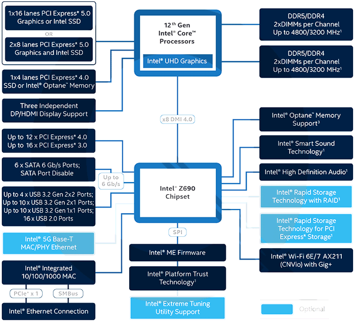
- Supports both DDR4 and DDR5, with standard data rates of at least DDR5-4800 compliant on four-module configurations.
- Will automatically use Gear 2 or Gear 4 modes for DDR5, running the memory controller at ½ or ¼ speed, depending on data rate.
- Retains 20 CPU PCIe lanes, but 16 of those are increased to PCIe 5.0 data rates.
- Uses DMI 4.0 to connect the CPU to the PCH (chipset) at PCIe 4.0 x8 speeds.
- New PCH has four more PCIe lanes, including 12 PCIe 4.0 and 16 PCIe 3.0.
- Supports up to four USB 3.2 2×2 (20Gb/s) ports.
- New CNVio modules support Intel Wi-Fi 6E, and possibly Wi-Fi 7.
- Uses “Big-Bigger” hybrid cores to improve thread handling while retaining 125W TDP.
- Lower stack height requires new CPU cooler bracket.
Gear 2 is utilized in this case, which means that the controller runs at half the frequency of the memory, resulting in considerable latencies. Gear 1 is also used in this case. It is also possible to use Gear 4 for the expected high speeds at which ddr5 is expected to operate, with the clock speed being reduced by half once more. In order to improve performance, the Direct Media Interface link is being upgraded from DMI 3.0 x8 to PCIe 4.0. Additionally, there are 5 and 1 gigabit Ethernet, four USB 3.2 gen 2x2 ports, and WiFi 6E and 7 standards. The overclockable K and KF models, as well as the Z690 chipset and the remainder of the Alder Lake lineup, are slated to be released on November 19, with the rest of the Alder Lake lineup debuting at CES 2022.
Socket LGA 1700 and coolers
Alder Lake-S also makes use of a new processor socket, the LGA 1700, which is designed specifically for it. It's noticeably larger than the LGA 1200 socket. The requirements for coolers have also altered as a result of the introduction of LGA 1700. Intel says little about this, but numerous manufacturers (including Noctua) have already announced that they will be releasing new mounting kits to complement their existing products. Corsair and EK Waterblocks have also announced LGA 1700 water coolers in the past few weeks. Intel itself claims to have revised the way the package is divided once more for the latest release. Core chips were used in the tenth and eleventh generations, and their thickness had already been lowered to ensure that heat could be better dissipated. The chip has been made even thinner for Alder Lake, and the soldering timing has been adjusted to account for this. The integrated heat spreader has only been thickened slightly, resulting in the processor as a whole remaining the same size in terms of thickness. This should result in improved cooling performance without requiring cooler makers to make too many modifications to their mounting techniques, which would be undesirable. The heatspreader btw is soldred top the CPU die.
Windows 11 and software schedulers: Intel Thread Director
In an effort to enhance performance while utilizing the least amount of energy, it is reasonable to assume that background operations will be performed on efficient cores and that highly utilized performance cores will be used for gaming and other applications such as video editing and editing. Alder Lake would be an excellent companion for Windows 11, which includes an efficient thread scheduler on the basis of which Intel has collaborated extensively with Microsoft for several years. Intel has stated that this lga1700 socket processor family will be released in the second half of this year. We anticipate that Windows 10 will function effectively with Alder Lake after some updates; however, Windows 11 may be more efficiently tuned in terms of thread scheduling in respect to workloads than Windows 10. The software implementation of the Hybrid Architecture was perhaps the most difficult aspect of the project. Until recently, the possibilities for intelligent job assignment to different types of cores were severely constrained. It was one of the few data points available to determine whether a process was operating in the foreground or the background; an intensive game will run on the fast cores, while a background task such as email synchronization will run on the frugal cores. This approach, however, requires more data to be applied on a broad scale in order to be able to make the most efficient decisions at all times, even in increasingly complex situations. Intel has created a hardware scheduler called the thread director, on its end it monitors the instruction mix of all current runtimes and sends input to the operating system. The software scheduler in Windows 11 is capable of interpreting this feedback and assigning the most appropriate processes to each type of core on a continuous basis.
