2 - Architecture
GeForce GTX series 200
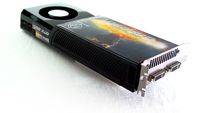
The product we review today is the GeForce GTX 280, a raw beast of a processor for sure.
The new GTX series 200 GPUs amounts up-to 1400 million transistors. It's the biggest goblin that NVIDIA has ever built, seriously, 1400 transistors means it's a freak on a leash. Think about that for a minute guys, and keep in mind that the GeForce 8800 'only' had roughly 700 Million processors. That's roughly doubling up the previous transistor count. Interestingly enough, that would also double up the die-size of the processor and so you'd expect NVIDIA to move to a smaller fabrication process for this graphics processor. They did not as the new architecture is still based on a 65nm fabrication size. The chip is being made at TSMC and according to them ... the biggest one they've ever made.
Unconfirmed info states that NVIDIA has come up with a huge die measuring 24 x 24 mm. And not many chips will actually fit on a 300 mm wafer, since , resulting in a die area size of 576 mm2. We measured and it's indeed easily 5.5 cm. I have no clue how a chip this big really yields, but this certainly is one expensive graphics processor to make. We expect NVIDIA to move to a smaller fab process (55nm) pretty soon.
Let's walk through some of the main features (you need to stamp into your head) of this new beast:
- 1.4 billion transistors
- 993 GigaFLOP processing power
- 240 processing (shader) cores (GTX 280)
- 192 processing (shader) cores (GTX 260)
- DirectX 10
- New power management enhancements
- CUDA parallel processing
- GeForce PhysX
So the thing you'll wonder about is, where are all these transistors going? Obviously a big chunk of the transistors are being utilized for the shader cores. And shader cores the product surely has, 240 of them on the GeForce GTX 280. The new shader architecture have some cool new features. Sitting in-between them now is a integration of local cache memory (16k software managed cache). It is sitting in-between a block with 8 shader cores. So simply put, what helps here is that the data / instruction doesn't have to leave the GPU anymore to crunch it's data (normally in the regular framebuffer memory. This is a very significant improvement in the architecture.
Let me show you some building blocks on that information. Light green, the shader cores, yellow the new 16k shared memory cache, brown texture filtering. As you can see the shaders are clustered in three blocks of eight shader processors. Then there are ten clusters totaling up towards the 240 shader units for the GeForce GTX 280. And if you do the math with me real quick then the GeForce GTX 260 has to have 8 shader clusters with a total of 192 shader processors.
Okay then people, it's time to get a little deeper under the hood and inside that thing we like to call the GPU. As you noticed, NVIDIA is actually released two products.
- GeForce GTX 280: 602MHz GPU, 240 shaders, 1296MHz shader processors, 1107MHz memory, 1GB memory, 512-bit memory bus, 141.7GB/s memory bandwidth, 48.2 billion/s texture fill rate
- GeForce GTX 260: 576MHz, 192 shaders, 1242MHz shader processors, 999MHz memory, 896MB memory, 448-bit memory bus, 111.9GB/s memory bandwidth, 36.9 billion/sec texture fill rate.
The cheaper GeForce GTX 260 will be priced at an interesting $449 and inevitably will fight with ATI's upcoming Radeon RV770/4870. The GeForce GTX 280 will be about 25 per cent faster than the 260, yet cost more with a steep $649 sales price.
The GeForce GTX 280 has a pretty amazing 240 stream processors and runs at a core clock frequency of 602MHz. There are more clocked domains inside that GPU though, the shader processor run at 1296MHz and the memory is at 1107MHz (effective 2214 MHz). All-in-all we feel the clocks are a little bit on the conservative side. The GTX 280 has eight 64-bit memory controllers, 8x 64-bit = 512 Bit.
This high-end part has 1GB of GDDR3 memory which has a 512-bit memory bus that binds to 8 memory controllers inside the GPU. At the end of the pipeline we run into an improved ROP (Raster Operation) engine, and the 280 has 30 of them.
All that brute transistor power results into roughly 933 GFLOPS of performance .A tad unexpected is to see that this card needs both a 6-pin and 8-pin power connector to get enough juice. NVIDIA claims a TDP (peak wattage) of roughly 235 Watts, which in all honesty is not even that bad considering the GeForce 8800 Ultra isn't that far off from that number either. And trust me when I say .. this puppy is roughly twice as fast.
| GeForce 8800 Ultra |
GeForce 9800 GTX |
GeForce 9800 GX2 | GeForce GTX 260 |
GeForce GTX 280 | |
| Stream (Shader) Processors | 128 | 128 | 128x2 | 192 | 240 |
| Core Clock (MHz) | 612 | 675 | 600 | 576 | 602 |
| Shader Clock (MHz) | 1512 | 1675 | 1512 | 1242 | 1296 |
| Memory Clock (MHz) x2 | 1080 | 1100 | 1000 | 999 | 1053 |
| Memory amount | 768 MB | 512 MB | 512 MBx2 | 896 MB | 1024 MB |
| Memory Interface | 384-bit | 256-bit | 256-bit | 448-bit | 512-bit |
| HDCP | Yes | Yes | Yes | Yes | Yes |
| Two Dual link DVI | Yes | Yes | Yes | Yes | Yes |
