Product Innards
Product Innards
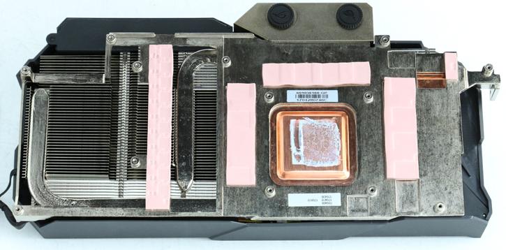
The hybrid cooling solution is impressive of course, it uses very thick heat-pipes that pass through a heatsink with the liquid cooling block on top. That's as good as it gets really, and sure, that shows in the great cooling performance.
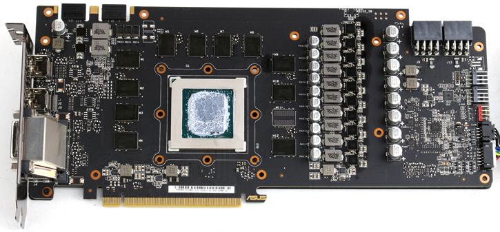
When we flip the PCB around you can also see the critical components are covered padding and is thus cooled as well as most ICs. ASUS applies padding on top of the GDDR5X ICs, the VRM area as well. The PCB itself is very clean and distinctively recognizable for ASUS.
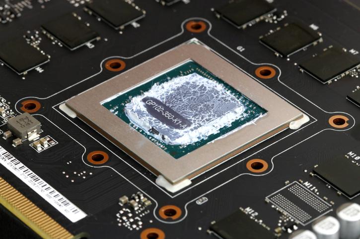
This is the GP102 graphics processor from Nvidia covered with thermal interface material. The Nvidia GP102 graphics processor is based on Pascal architecture at a 16 nm process at TSMC. This bad boy has a transistor count of 12 billion and do not underestimate the die size, that is 471 mm² you are looking at.
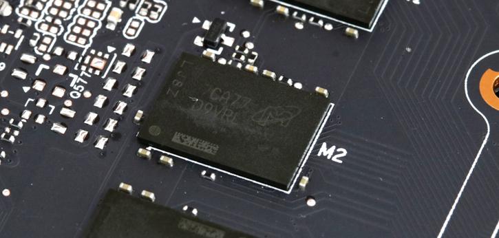
The GDDR5X memory chips are made by Micron and are specced to run at 11,000 MHz GDDR5 (effective data-rate). Tweaked, you are looking at a capability of roughly 12,000 MHz (effective data-rate). These are Micron D9VRL rated at 11 Gbps / 1.35V, however Micron also offers new 12 Gbps IC under the product name D9VRN which still have not been used for 1080 Ti (only 1080).
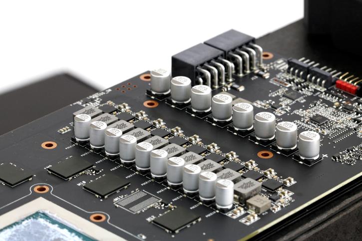
You can count along with me, ten phases for the graphics proc. We'll look at the voltage regulator as well. BTW, above you can also see an empty SMT trace for one more memory IC. This is an 11 GB product, 12 GB would be possible. Across the PCB you see a clean component layout which includes premium VRM components. You can see SAPII (the graffiti style) chokes, that would be a molded indicator (chokes). These concrete alloy chokes help decreasing buzzing noises. And the the square chips to the right are SAP mosfets, for ASUS they use DrMOS.
And to the left upper segment of the PCB, two more thus two phases for the memory subsystem. You can also see a couple of POSCAPs, aka Conductive Polymer Tantalum Solid Capacitors, these are the ones that light up and reach high temps.
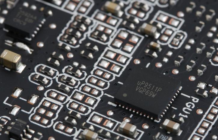
Voltage phase management then - ASUS uses the uPI based uP9511P voltage regulator, a recent and much used model voltage controller for many NVIDIA GP104 GPU based graphics cards. uP9511 can be configured in 8/7/6/5/4/3/2/1-phase operation and if you counted with me there are 10 of them + 2 for memory. So how does ASUS get to 12 phases? Well, look at the next photo.
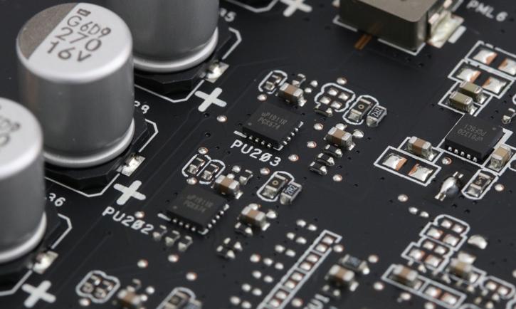
We spot two Up9511 phase doublers, hence in this case ASUS might be using Up9511 in a 5-phase configuration and using other UPI semiconductor uP1911R ICs as doublers to get their 8-phases for the GPU and then two to memory. This is common on many graphics cards, these feed into other power stages.
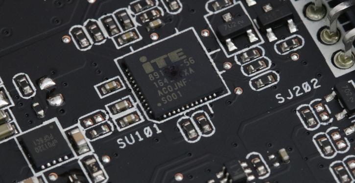
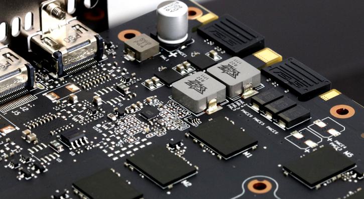
Situated a little higher we can spot an ITE 8915FN, this chip is used for monitoring and manage the current of the graphics card.
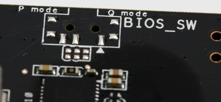
And yeah, somehow the dual-bios did not make it!, I guess this card doesn't need a Q / Quiet mode BIOS switch ;-)
