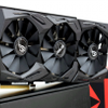
Product Innards
Product Innards
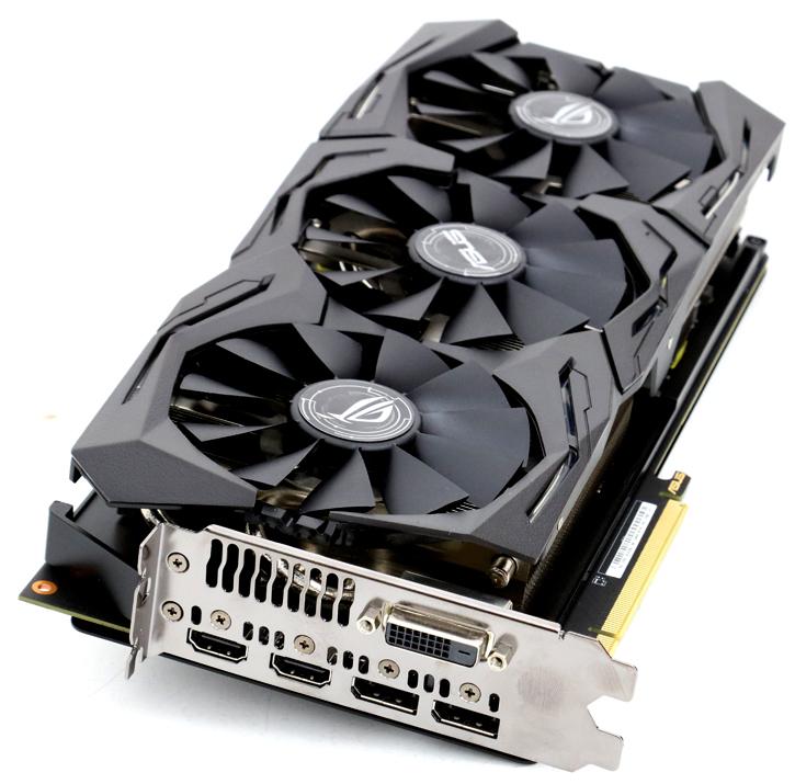
Right, lets strip her nekked and see what is going on at the PCB components wise.
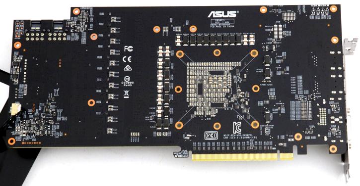
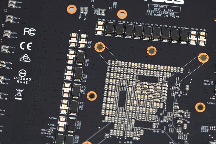
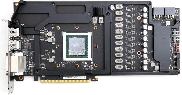
So, we take off the back-plate locked in with screws. At the backside there is a gap between the components and back-plate through the use of riser standoffs. Let's immediately zoom in at the upper array of PC marking above the rear side GPU spacing
Later in this review you will see on the thermal image pages that the backside and upper part of the card lights up extensively. Well, on the opposing side, as part of the VRM design ASUS makes use of POSCAPs, aka Conductive Polymer Tantalum Solid Capacitors, these are the ones that light up and reach high temps.
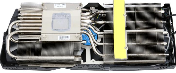
The cooling solution is impressive overall, it uses six heat-pipes that pass through a heatsink, with thermal paste tied to the all-copper yet nickel plated block. That's as good as it gets really, and sure, that shows in the great cooling performance. All critical compoents have been thermally padded.
When we flip the PCB it around you can also see that the critical components are covered with a full contact plate (padding underneith as well). The DrMOS integrated power stages have padding and thus is cooled as well as most ICs.
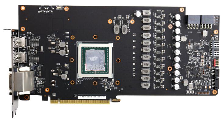
With the heatplate removed we now have the full PCB visible, what an incredible clean PCB. Lots of space as hey, there's no GDDR5(X) memory mounted. This is a very clean PCB design alright. Let's run thorugh some of the components.
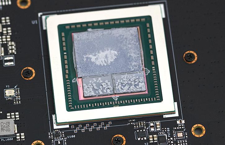
First and foremost, here we have the Vega 10 graphics processor from AMD with its 4096 Shader Cores. I left the thermal compound on there as part of the testing so you can see how it is applied as well as I need to re-assemble the card fast for further testing for a following FCAT review), but all tests have been performed PRIOR to disassembly of the card. At the lower GPU side you can see the two HBM2 stacks, each 4 GB. You'll notice that this Vega 64 GPU one we have seen before, the version without the molding epoxy and the lower sitting HBM2 stacks. You can tell from the thermal compound (the dot effect on the HBM2) that the memory contact surface area is not optimal.
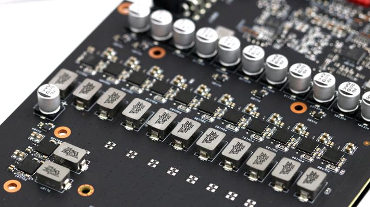
You can count them, 12+1 phases. Likely 12 for GPU power delivery and then a dedicated memory power phase. We'll look at the voltage regulator as well.
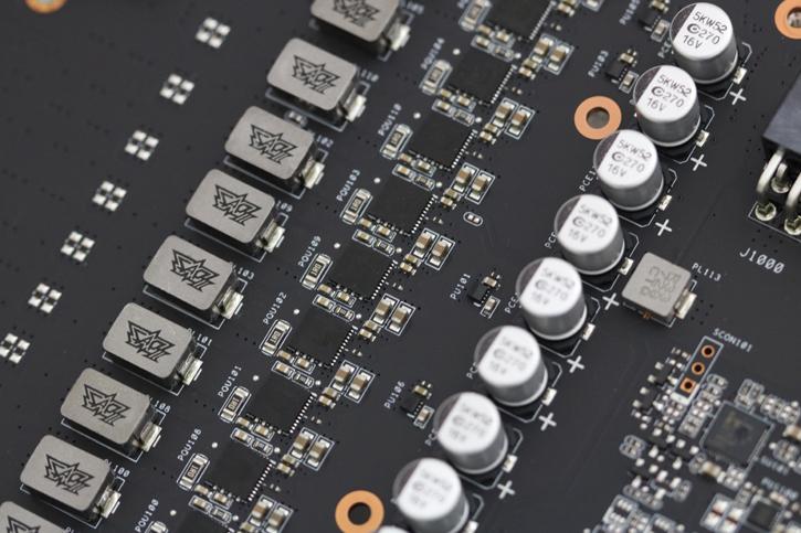
Across the PCB you see a clean component layout which includes premium VRM components. You can see SAPII graffiti style chokes, that would be a molded indicator (chokes). These concrete alloy chokes help decreasing buzzing noises.
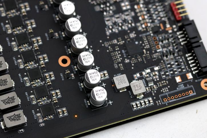
The the square chips to the left of the capacistors are SAP mosfets, for ASUS always uses DrMOS. We stumble into 5K SAP capacitors (which offer a longer lifespan compared towards normal capacitors ).
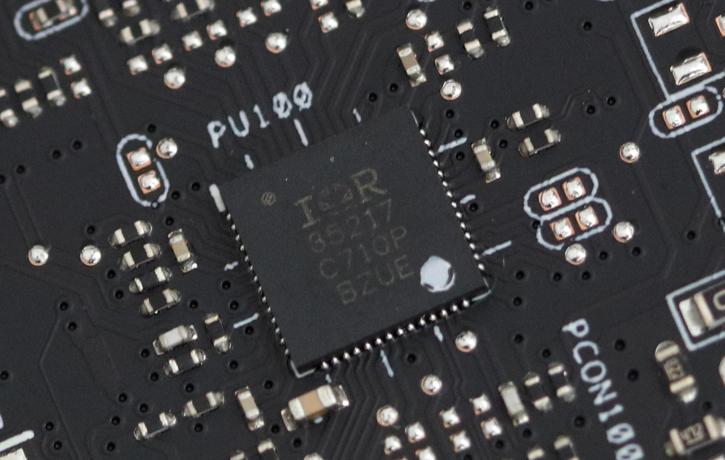
ASUS is using an International Rectifier IR35217 power controller, a fairy undocumented 8-channel multi-phase controller that can provide six phases for the GPU and another two for say memory. If you have had a sharp eye, you'll notice ASUS thus must be doubling GPU phases. This is common on many graphics cards. So it's 6 phases, but doubled up to 12.
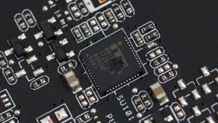
Situated a little higher we can spot an ITE 8915FN, this chip is used for monitoring and manage the current of the card.
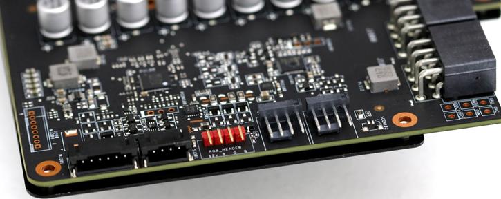
Here we can see ASUS ASUS FanConnect II controlled fan headers that you can use, to the left of it an RGB header, which can be controlled with Aura. The two most right connectors are for the internal board fan and RGB.
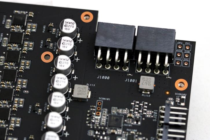
Next to the two 8-pin power headers you can spot a number of several voltage and modification points (VDDCI, MVDD, VDDC, OVCI, OVM, OVC) slash ROG Connect soldering points.
