Product Photos
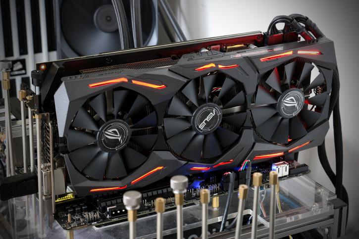
The card based on reference clocks can manage to ooze out roughly 12.66 TFLOPS in single precision (fp32) performance (based on AMD claims / measurements). The Vega 10 GPU is based on a 12.5 billion transistor GPU and is fabbed on a 14nm FinFET LPP process. It comes with over 45MB of SRAM cache across the chip and thus holds either an 8 GB (consumer) or 16 GB (Pro) configuration. Radeon RX Vega is rated at a 295 Watt total board power and has 64 CUs x 64 shader processors per CU (= 4096 shader processors). Above, the cooler and cooling design. You are going to spot two 8-pin power connectors that feed the power phase design.
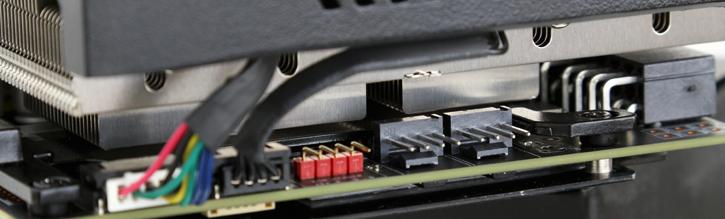
That RGB setup of the card can be managed with Aura software and other hardware as well the extra four-pin Aura RGB header alongside FanConnect II for further expansion that is on-board of this card as you can see in the photo above. That is located at the rear side of the card.
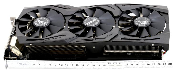
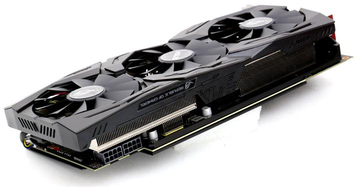
The STRIX model tested is an air-cooled dual-slot based unit with three fans, it sizable though at almost 30cm in length. Basically the design can deliver ~300 Watts through the connectors and then another 75 Watts is fed though the PCI-Express slot (depending on how the phase distribution is configured). In theory this means there is plenty left for GPU and memory tweaking.
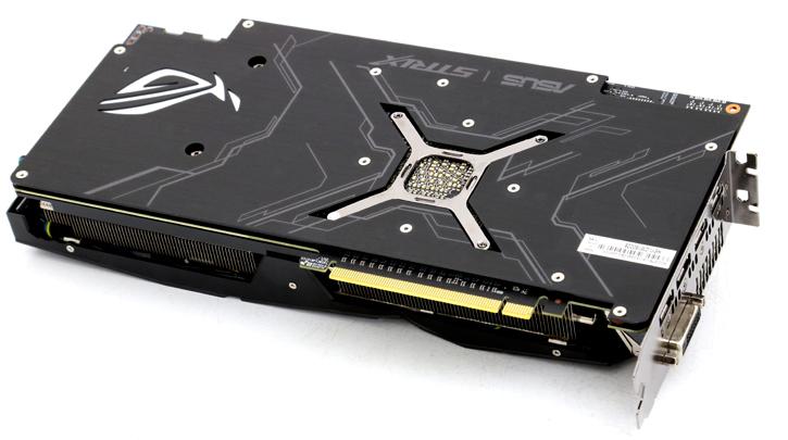
As stated, monitor display outputs include two DisplayPort 1.4 connectors and two HDMI 2.0b outputs. Overall the card design is more of the same in terms of aesthetics. Nice looks overall though.
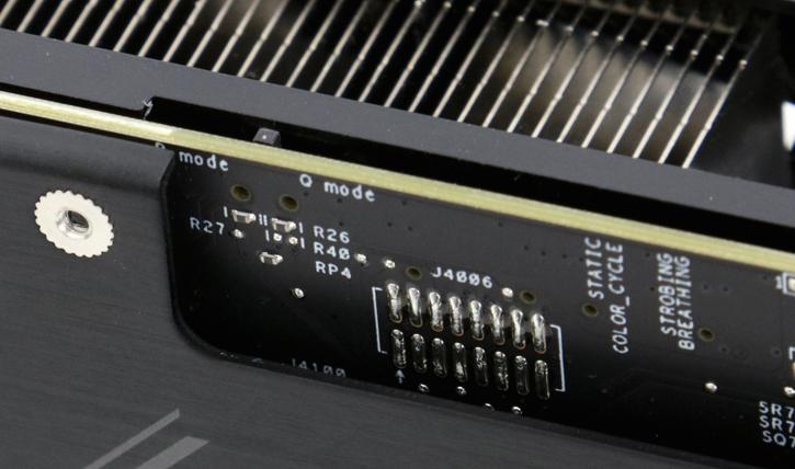
At the front top side you can select a BIOS preference, there will be energy efficiency choices to be made for the secondary BIOS. So the alternative mode should be slightly more energy efficient. We doubt that anyone will use that mode as you do not purchase the most high-end card to reduce performance, however it is nice to have a fail-safe BIOS on-board of course. We test defaults, always.