The AMD 880G chipset
The AMD 890G Chipset
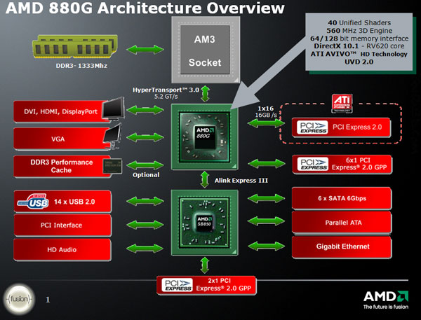
So to understand this chipset from AMD, aimed at the more budget conscience PC user, all we simply need to do is tell you a thing or two about its features. The AMD 800 series chipset consists out of two chips that are added onto the motherboard PCB. The Northbridge chip, which is called the 880G and the paired (Southbridge chip) SB850. Together they form the infrastructure for all standard devices, connectivity and interconnect bandwidth.
The Northbridge chip primarily functions as a control HUB for your processor, memory and PCIe links towards your graphics chipset. It is the primary chip responsible for these functions, the FX (opposed to G) extension however indicates that there is no IGP embedded into this ASIC which the G and GX versions do have.
The 880G has sufficient PCIe links available for your dedicated graphics (or other add-in cards), but is trimmed down though. The chipset allows you to utilize two full x16 graphics cards. But install one and it can utilize x16 PCIe lanes, install two and it will split into a X16 and a x4. So there's no real crossfire support to be found here, unless you sincerely limit bandwidth.
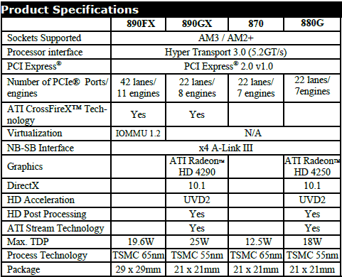
AMD now has a pretty extensive lineup of series 800 motherboards ready. The 890GX and FX chipsets, the 870 and the 880G chipset. Below you can find a little chart showing the difference without hogging up a full page with explanations.
As stated this chipset also includes native support for SATA 6Gb/s for aggressive RAID and SSD configurations and most motherboards are expected to include USB 3.0 support, employing the chipsets dedicated PCI express link and leading discrete USB 3.0 solutions.
The G series (opposed to FX) extensions however also means that there's an IGP embedded into this ASIC. Much like the 785 chipset the 880G has a GPU tucked nicely away into the die. It's based off the Radeon HD 4200 silicon, the Radeon HD 4250 to be precise, which is slightly slower clocked than the 890GX. ASUS arms the IGP with an optional 128MB cache partition called sideport to give it a little more breathing space.
Games wise, a simple game or two could be played fairly okay in lower resolutions. It's powerful enough for the low-level stuff, but for anything a little more serious you'll of course need a dedicated graphics card. The embedded DX10.1 IGP (RV620) still packs 40 shader processors with a core and shader clock at 560 MHz. This solution will be faster than the IGP Intel's Clarkdale processors for example, have embedded. It works fine for HTPC and desktop usage, but for gaming obviously you'll need a real dedicated graphics card.
Being a series 4000 graphics core, it will open up ATI Stream technology, which means you can encode media files over the GPU with 3rd party software like MediaShow Espresso or even accelerate Adobe Photoshop and Adobe flash. Latest additions to the IGP support, now also include Accelerated flash support and WMV acceleration.
In the 890 FX chipset we spot IOMMU support, not in the 880G though and not something that the majority of you guys would be interested in, but it allows for virtual addressing of memory by system devices. This enables devices to use their native drivers in a virtualized environment for enhanced performance. In a non-virtualized environment, IOMMU provides memory isolation and protection capabilities - device access to system memory is vetted by the IOMMU such that critical/unrelated memory information (e.g. kernel pages, protected content ) can be protected, leading overall to a more robust system.
With an updated Hyperlink (revision 3) we now can connect to the SB850 chip with a well-appointed 2GB/sec bandwidth (full-duplex). Let's have a look at the SB850 Southbridge chip.