Specs and overview
After the GTX 480 release NVIDIA went back to the drawing board and introduced a new revision based on the GF100 ASIC, now labeled as the GF110, used on the GeForce GTX 580.
With this release, NVIDIA has a full range of products out on the market from top to bottom. All the new graphics adapters are of course DirectX 11 ready. With Windows 7 and Vista also being DX11 ready all we need are some games to take advantage of DirectCompute, multi-threading, hardware tessellation and new shader 5.0 extensions. DX11 is going to be good and once tessellation kicks into games, much better looking.
- GeForce GTX 580 : 512 Shader Processors, 384-bit memory interface, 243W TDP
Let's put most of the data in a chart to get an idea and overview of changes:
| Graphics card | GeForce GTX 480 | GeForce GTX 580 | ASUS GTX580 DCUII |
| Fabrication node | 40nm | 40nm | 40nm |
| Shader processors | 480 | 512 | 512 |
| Streaming Multiprocessors (SM) | 15 | 16 | 16 |
| Texture Units | 60 | 64 | 64 |
| ROP units | 48 | 48 | 48 |
| Graphics Clock (Core) | 700 MHz | 772 MHz | 782 MHz |
| Shader Processor Clock | 1401 MHz | 1544 MHz | 1564 MHz |
| Memory Clock / Data rate | 924 MHz / 3696 MHz | 1000 MHz / 4000 MHz | 1002 MHZ / 4008 MHz |
| Graphics memory | 1536 MB | 1536 MB | 1536 MB |
| Memory interface | 384-bit | 384-bit | 384-bit |
| Memory bandwidth | 177 GB/s | 192 GB/s | 193 GB/s |
| Power connectors | 1x6-pin PEG, 1x8-pin PEG | 1x6-pin PEG, 1x8-pin PEG | 2x8-pin PEG, |
| Max board power (TDP) | 250 Watts | 244 Watts | 249 Watts |
| Recommended Power supply | 600 Watts | 600 Watts | 600 Watts |
| GPU Thermal Threshold | 105 degrees C | 97 degrees C | 97 degrees C |
Now, at the end of the pipeline we run into the ROP (Raster Operation) engine and the GTX 580 again has 48 units for features like pixel blending and AA.
There's a total of 64 texture filtering units available for the GeForce GTX 580. The math is simple here, each SM has four texture units tied to it.
- GeForce GTX 470 has 14 SMs X 4 Texture units = 56
- GeForce GTX 480 has 15 SMs X 4 Texture units = 60
- GeForce GTX 580 has 16 SMs X 4 Texture units = 64
Though still a 40nm based chip, the GF110 GPU comes with almost 3 billion transistors embedded into it. The TDP remains the same at roughly 240~250 Watts.
What about the tested card ?
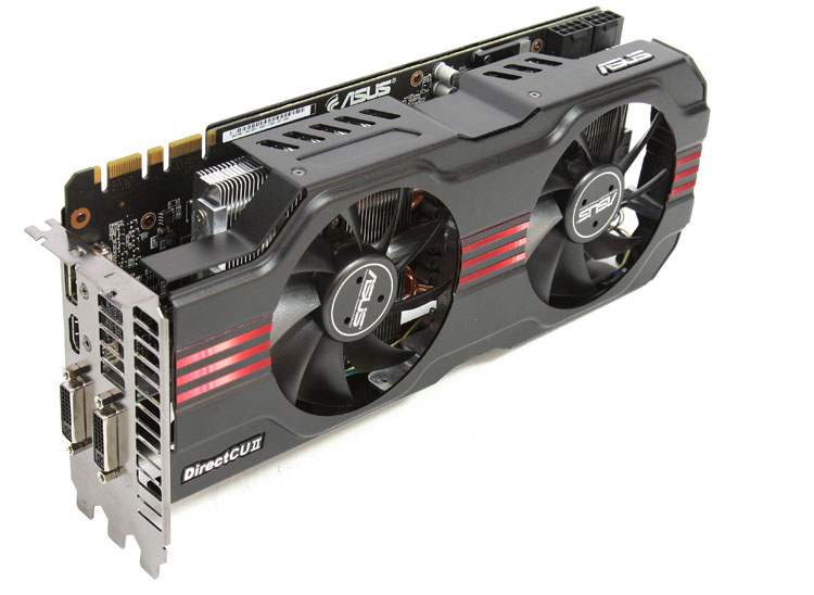
So then, the ASUS GeForce GTX 580 DirectCU II has an enormous triple-slot cooling system, in addition to a custom PCB (printed circuit board). The cooler makes use of three copper heatpipes, all of which make direct contact with the GPU and VRM sections, oooh and it has two 100 mm fans.
The card itself comes with an 8-phase VRM (+2 for memory) design which draws its juice from two 8-pin PCI Express power connectors (and yes in SLI that means four 8-pin power headers (!)). The card's PCB is custom and next to a more advanced circuitry it also comes with the better quality components. Amongst others we spot a proadlizer made by NEC, whose purpose is to manage the power supplied to the GPU and filter it more clean.
Being a GeForce GTX 580 graphics card this particular model has 512 shader processors and 1,536 MB of GDDR5 memory running over a memory interface of 384 bits wide connecting to that GF110 GPU.
The clock speeds set at 782 MHz on the core, 1564 MHz on the shader processor domain and 4008 MHz (effective data-rate) on that gDDR5 memory. Connectivity wise you'll get a DisplayPort and an HDMI output, in addition to two DVI connectors.
Today we'll put two of these in tandem, yep SLI.