Ryzen Processors and X570 chipset
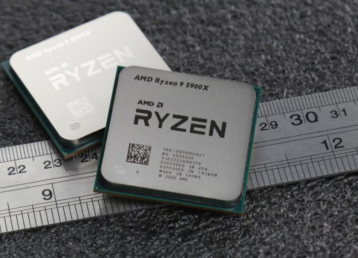
Ryzen Series 5000 for Desktop
A revised naming schema. AMD validated that the ZEN3 (internal codename Vermeer) based processors are called the Ryzen 5000 series. And that brings the Mobile APU and Desktop lineup in the same numbering. This will clarify the confusion between the numbering for mobile parts and desktop and bring that numbering in line with the motherboard chipsets from an identifiable point of view (Series 500). AMD has now explained this itself for the codename Vermeer products. AMD announced the processors are based on the Zen 3 architecture and, like the CPUs based on Zen 2, are fabbed at 7nm. Of course, ZEN3 will find its way through the entire AMD family of products, from top to bottom mobile, desktop, but in summer 2021, we also expect ZEN3 based Threradripper SKUs. You have to begin somewhere, and initially released are:
- Ryzen 5 5600X (6c/12t)
- Ryzen 7 5800X (8c/16t)
- Ryzen 9 5900X (12c/24t)
- Ryzen 9 5950X (16c/32t)
 |
|||||
| Processor | Cores / Threads | Clock speed/turbo (GHz) | Cache (total) | PCIe lanes CPU+x570 chiplet) |
MSRP |
| Series 5000 | |||||
| Ryzen 9 5950X | 16/32 | 3.4 / 4.9 | 72MB | 40 | $799 |
| Ryzen 9 5900X | 12/24 | 3.7 / 4.8 | 70MB | 40 | $549 |
| Ryzen 7 5800X | 8/16 | 3.8 / 4.7 | 36MB | 40 | $449 |
| Ryzen 5 5600X | 6/12 | 3.7 / 4.5 | 35MB | 40 | $299 |
| Series 3000 | |||||
| Ryzen 9 3950X | 16/32 | 3.5 / 4.7 | 72MB | 40 | $ 749 |
| Ryzen 9 3900XT | 12/24 | 3.8 / 4.7 | 70 MB | 40 | $ 499 |
| Ryzen 9 3900X | 12/24 | 3.8 / 4.6 | 70MB | 40 | $ 499 |
| Ryzen 7 3800XT | 8/16 | 3.9 / 4.7 | 36MB | 40 | $ 399 |
| Ryzen 7 3800X | 8/16 | 3.9 / 4.5 | 36MB | 40 | $ 399 |
| Ryzen 7 3700X | 8/16 | 3.6 / 4.4 | 36MB | 40 | $ 329 |
| Ryzen 5 3600XT | 6/12 | 3.8 / 4.7 | 35MB | 40 | $ 249 |
| Ryzen 5 3600X | 6/12 | 3.8 / 4.4 | 35MB | 40 | $ 249 |
| Ryzen 5 3600 | 6/12 | 3.6 / 4.2 | 35MB | 40 | $ 199 |
| Ryzen 3 3300X | 4/8 | 3.8 / 4.3 | 18MB | 40 | $ 120 |
| Ryzen 3 3100 | 4/8 | 3.6 / 3.9 | 18MB | 40 | $ 99 |
For the time being, Ryzen Series 3000 and 5000 will co-exists next to each other. However, with time passing by, we do not doubt that series 3000 will phase out at one point. But let's talk a tad more about architecture changes.
A unified 8-core design
We explained that the solution at hand for that increased gaming performance was twofold; I already explained the first. A second solution to bypass any performance degradation in gaming is to eliminate inter-core and inter CCX latencies. ZEN2 addressed that, to some extent, with a few efficiency solutions to be found at cache levels. However, of course, getting rid of the inter-core complex partition latencies is another thing. ZEN3 stepped away from that two core complex (CCX) of 4 cores per die (CCD). The architecture is now a single core complex of 8 cores per die (CCD), and that is an easy win in latency as all cores can access the same L3 cache.
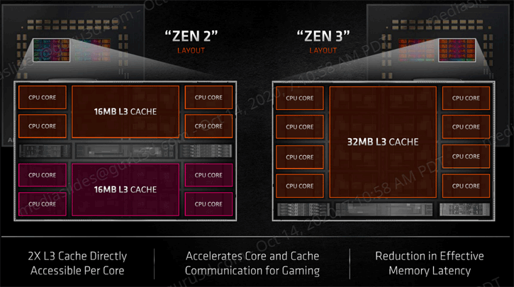
So I know reading this all might be confusing to that common PC consumer or gamer, but let me try and break it down simple for you. Zen 3 will continue to use an MCM (multi-chip module), or chiplet design; it will use two CCDs (a die holding CPU cores) and one I/O die. There will only be one CCX (cluster of processor cores) per CCD, and this CCX thus consist of eight cores, e.g., 1x8, which was 2x4 in previous generations. The benefit here is that a total of 32MB of L3 cache can now be accessed directly with ZEN3 (ZEN2 had 16MB per CCX, thus per four cores). That L3 cache pool is shared across all eight cores in the CCX, and gone are thy latencies. So yes, Zen 2 offered 32MB of L3 cache per CCD, but that had to be shared between the two CCX complexes effectively-being that was 2x 16MB. There's also 512KB of L2 cache per core within the CCX, for a total of 4MB of L2 cache per CCD. Overall, IPC performance improvements are rated to hit roughly 19% per thread. You can add to that clock frequency and Turbo bins seen over ZEN2; that number might end up being 20 to 25% accumulated.
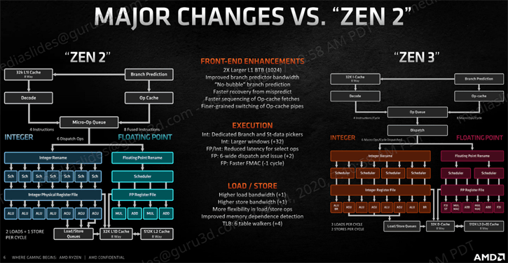
It's not just that '8-core cluster' responsible for all the IPC increase; many variables come into play at a deeper architecture level, including Advanced Load/Store Performance and Flexibility Wider Float and Int Engines and what is referred to as “Zero Bubble” Branch Prediction. The L1 instruction cache is 32kB. The L2 cache is also the same 512kB per core; the L3 cache is 32MB instead of 2x16MB. The instruction cache contains the x86 instructions that are retrieved from the memory for processing. However, by giving this cache more inputs and outputs, an 8-way associative instead of a 4-way associative will make up for that design choice. Also, by optimizing algorithms for pre-fetching instructions and increasing the caches at other levels (like the L3 cache), the smaller instruction cache effect is limited. Zen supported 128-bit, Zen 2 moved towards 256-bit, which brings us to support for AVX2 instructions; these can be processed in one single clock-cycle now. Zen3 does not yet support AVX512. Load/store units have been optimized further from offering 2 loads + 1 cycle per store, now offering 3 loads and 2 stores per clock cycle. And all these things combined increase that overall IPC.
- Up to 8 cores that can run in single-threaded mode (1T) or two-threaded SMT mode (2T) for a total of up to 16 threads per complex.
- 4MB L2 cache per CCD with 512 KB L2 cache per core.
- Up to 32MB L3 cache shared across all cores within the complex.
7nm production -- From AMD's materials, which stated "7nm+," it was initially assumed by the media that the 7nm process would be the new EUV (extreme ultraviolet) lithography from TSMC (N7+). A shift to N7+ would be expected to lower power consumption by 10% and offer up to a 20% increase in transistor density. This would also allow for higher clock speeds at the same power consumption.[4] AMD has clarified that they did not mean any specific process by "7nm+" and that they would be using an improved version of 7nm (N7), which includes the possibility of the DUV (deep ultraviolet) N7P process or some other unnamed process.
DDR4 memory support
DDR4 memory support will not be very different from the previous generation with one remark made. On ZEN2, as soon as you go higher than DDR4-3733 MHz, a 2:1 multiplier will kick in for the Infinity Fabric (the interlink in between the processor die and IO chip, which starts working at half the memory clock frequency. That 2:1 multiplier switches on at DDR4-3733, which would affect the speed at which the various core complexes within the CPU can communicate with each other. For the best overall system performance, AMD, therefore, recommended DDR4-3600 speed. For ZEN3, this is slightly different as the clock frequency of that interlink was raised a notch and can now support 4000 MHz without the IF limiter kicking in. DDR4-3600 is the price/performance "sweet spot" and remains AMD's recommendation for the Zen 3-based processors. However, the new optimum is DDR4-4000 with a synchronous IF or fabric clock (FCLK) and memory controller clock (ULCK) of 2,000 MHz.
Chipset compatibility
ZEN3 based Ryzen 5000 series processors will be drop-in compatible with the Series 500 chipset motherboard like the B550 and X570 (you'll need the latest available BIOS, of course). There will also be Series 400 chipset support for motherboards that have a 32MB BIOS. In short, for Ryzen 4000, aka ZEN3 processors that are released, it is recommended to have a B550 or X570 motherboard. With motherboards like B550 and X570, you are guaranteed to get optimal support for Zen 3 processors when they get released. Much like before, support will be added through firmware updates that motherboard manufacturers will make available and already made available by many manufacturers. Please check their website for BIOS updates. Initially, AMD had no plans to introduce “Zen 3” architecture support for older chipsets. While they wish could enable full support for every processor on every chipset, the flash memory chips that store BIOS settings and support have capacity limitations. So on the Series 400 chipset, you need to have 32MB BIOS storage; please check this with your manufacturer. Starting January 2021, they will introduce Ryzen 5000 support on selected motherboards in the B450 and X470 range.
Ryzen 5000 delivers 24 lanes PCIe 4.0
Ryzen 5000 CPUs will have a total of 24 PCIe Gen4 lanes. Four out of the twenty-four are used for the interconnect to the motherboard chipset, leaving 20 lanes Gen 4.0 for other utilization. 16 lanes (PCIe x16) are intended for graphics cards that are connected as x16 or two at x8. Seen from Gen 3.0 one a Gen 4.0 x8 link would offer similar to PCIe 3.0 x16 bandwidth. Four more PCIe lanes from the CPU are designed for fast storage such as PCIe 4.0 NVMe compatible SSDs. In addition to all that, a sidenote - AMD has integrated USB 3.2 Gen2 support into the CPU, which means you get four 10 Gbps USB ports at SuperSpeed. We'd recommend you to pair Ryzen 5000 with a B550 motherboard. However, if you have an urge for multiple PCIe Gen 4 capable NVMe M2 units, X570 is the choice to make as the X570 chipset delivers another 16 lanes PCIe 4.0. Per motherboard, things are going to be connected differently. PCIe slots, M.2 SSDs, LAN, card readers or WiFi modules are to be connected via the new interface standard. The configuration depends on the respective motherboard. Unlike the X370 and X470, the AMD X570 chipset was designed by AMD themselves and here's an interesting fact, the I/O chip that is mounted on the Ryzen 3000/5000 processors and the AMD X570 chipset are in fact the same chips, CPUs make use of the Global Foundries 12nm version and the X570 chipset variant is the same thing, just fabricated on a 14nm process. Since the processor actually has that 12nm IO chip, which is the same as the X570 chipset, it will also offer 4x USB 3.2 Gen 2 (Superspeed 10 Gbps) ports.
|
| ||||||
|---|---|---|---|---|---|---|
| PCIe Version | Line Code | Transfer Rate | x1 Bandwidth | x4 | x8 | x16 |
| 1.0 | 8b/10b | 2.5 GT/s | 250 MB/s | 1 GB/s | 2 GB/s | 4 GB/s |
| 2.0 | 8b/10b | 5 GT/s | 500 MB/s | 2 GB/s | 4 GB/s | 8 GB/s |
| 3.0 | 128b/130b | 8 GT/s | 984.6 MB/s | 3.938 GB/s | 7.877 GB/s | 15.754 GB/s |
| 4.0 | 128b/130b | 16 GT/s | 1.969 GB/s | 7.877 GB/s | 15.754 GB/s | 31.508 GB/s |
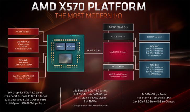
X570 PCH actually includes sixteen PCIe lanes, in addition to the 24 PCIe lanes on the CPU, with a total of 4 (four) 4-lane physical interfaces (4x PCIe 4.0 x4 PHY), fully configurable in PCIe x16, x8, x4, x2, x1, and SATA modes. The X570 chipset offers 8x USB 3.2 Gen 2, 4x USB 2.0, 4x SATA, and 8 separate PCI-Express 4.0 lanes. That leaves eight flexible lanes that can be used for PCI-Express and SATA. As you can see, the flexible design allows motherboard manufacturers lots of options in what they want to offer. When you think about it, an AMD X570 motherboard could even get four M.2 slots for PCI-Express 4.0 x4 SSDs. Please do keep in mind that only processors from Ryzen 3000 (Zen2) and newer will open up X570 to the CPU at PCIe 4.0 x4. If an older Ryzen family proc is used or, say, an APU based on older Zen1 architecture, the chipset connection will become PCIe 3.0. In the end, the X570 platform will be AMD's most advanced offering ever. It is leading over what Intel offers. The downside of all this new technology is that the motherboards are more complicated and expensive to fabricate.
Of course if one PCIe Gen 4 NVMe SSD is plenty enough for you, we'd advise B550. And if you are fine with PCIe Gen 3.0, honestly after January 2021 look for a nice B450 or X470 motherboard. The processor and memory performance will not be any different on all platforms. There's a lot of value to be gained by making clever choices here.
