Article Page 2
The APU for socket FP4 is produced in a BGA-type package. A new feature of these products will be an integrated Fusion Controller Hub (FCH) with PCIE 3.0, 2 SATA 6GB/s ports and 12 USB ports, including 4 ports with USB 3.0 support. The FP4 chips will be used in mobile computers and other low power devices with a power envelope of 15 to 35 Watt. New high density design libraries allowed AMD to fit 29 percent more transistors on Carrizo – 3.1 billion – in nearly the same chip size as the previous generation, Kaveri APU. This density increase has allowed a larger area for graphics, multimedia offload, and integration of the “Southbridge” system controller on a single-chip.
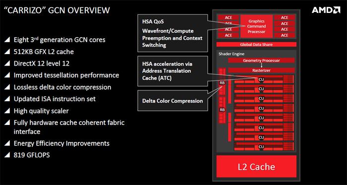
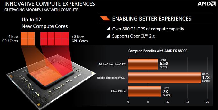
If we focus in on the GPU part, then we can see that AMD bumped up the architecture to Radeon Series 7 with a GCN 1.3 based architecture. A fullly enabled cluster will enable 512 Shader processors, DirectX 12 compatible offering roughly 819 GFLOPS of performance, which certainly is a good number for an integrated GPU. We'll get to specs and clock frequencies in a later slide. The GPU will get its own dedicated power supply again to adapt to energy efficiency.
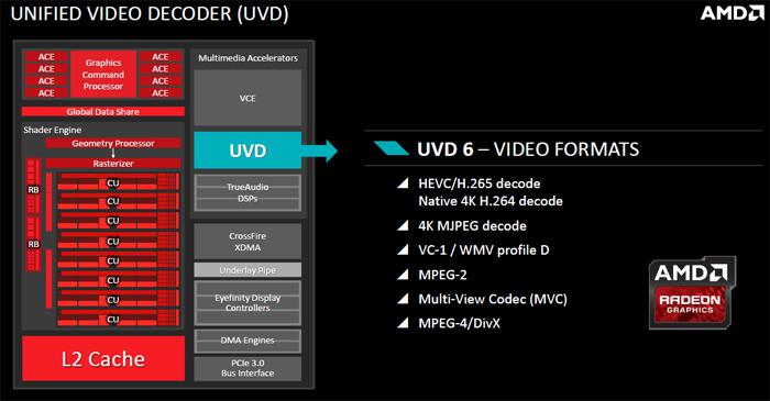
The increased support for multimedia includes the new, high-performance H.265 / HEVC video standard and double the video compression engines of its predecessor. The inclusion of H.265 in hardware will support true 4K resolutions, help extend battery life, and reduce bandwidth requirements when viewing compatible video streams.
The 6th Gen AMD A-Series products
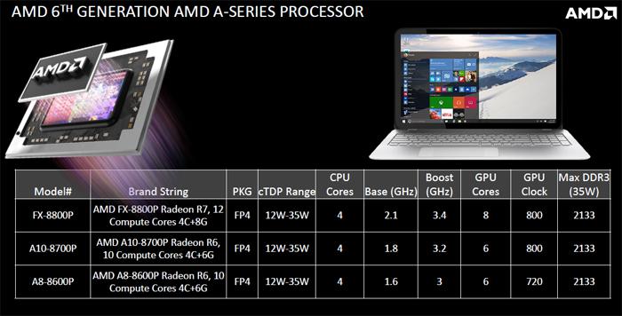
Desktop Carrizo is not yet announced, but for the Mobile segment initially three APU series will be released today. The products you will learn to know as the 6th generation A-series, and will be featuring revised AMD badges to indicate this. AMD will be retaining the current FX/A10/A8 branding with “6th generation” branding on the badges.
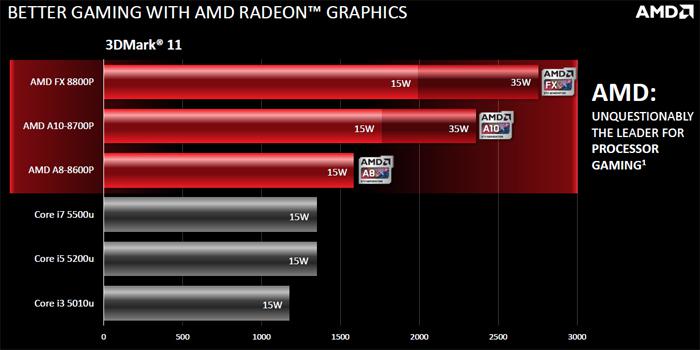
The top dog model is the FX-8800P running an upto 3.4 GHz clock frequency with a 2.1 Ghz base clock. It has four CPU cores and eight fully enabled Radeon R7 graphics cores clocked at 800 Mhz with 512 Shader processors). The TDP range is 12 to 35 Watt.
The A10-8700P will have a 1.8 Ghz base clock that can turbo towards 3.2 GHz. It has four CPU cores and eight fully enabled Radeon R6 graphics cores clocked at 800 Mhz each with 384 Shader processors). The TDP range is 12 to 35 Watt.
The entry level model will be the A8-8600P, it has a 1.6 Base clock with boost cpacity to 3 GHz. Despite earlier rumors it still has has four CPU cores and six Radeon R6 graphics cores clocked at 720 Mhz each with 384 Shader processors). The TDP range is 12 to 35 Watt.
And that concludes this little preview of Carrizo. We hope to review a kit soon enough, if the claims are right then the architecture should be sound for the mobile platform alright. It's a little puzzling to see that a 28nm would be able to pull this off in terms of perf per watt, but we'll gladly test that for you guys of course. Initial perf resutls definitely seems to indicate a good improvement over what the current gen solutions offer.
Live from Computex 2015, this is Hilbert signing out ..
