Architectural Details
Up-to 40 MB L2+L3 Cache
The caches; all parts are based on the same architecture, anything Ryzen. And considering there is 20 MB for an 8-core processor for the L2 and L3 cache, that can be multiplied by two and thus comes to 40MB of cache on the 16-core part.
 |
||
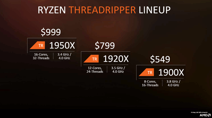
| Ryzen Threadripper 1950X | Ryzen Threadripper 1950X | |
| TDP | 180W | 180W |
| Core Topology | 4+4 (die 0) / 4+4 (die 1) | 3+3 (die 0) / 3+3 (die 1) |
| L2 Cache | 512K per core (8MB total) | 512K per core (6MB total) |
| L3 Cache | 16MB per die (32MB total) | 16MB per die (32MB total) |
| Base Frequency | 3.4 GHz | 3.5 GHz |
| All Core Boost | 3.7 GHz | 3.7 GHz |
| Boost Frequency | Up to 4.0GHz boost (4 cores) | Up to 4.0GHz boost (4 cores) |
| XFR Requency | Up to 4.2GHz XFR (4 cores) | Up to 4.2GHz XFR (4 cores) |
| SMT | 32 threads | 24 Threads |
| PCIe Gen3 Lanes | 64 | 64 |
 |
||
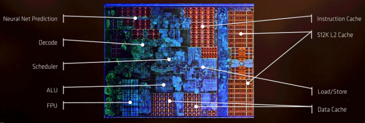
The 16-core part with four four-core CCX units aka Summit Ridge aka RYZEN in the end gets a per core L1 data cache size of 32 KiB, a L1 instruction cache size of 64 KiB and then a L2 cache size of 512 KiB per core.
- L1 16 x 32 Kb Data
- L1 16 x 64 Kb Instruction
- L2 16 x 512 Kbytes
- L3 4 x 8 Mbytes L3
The 12-core part with four three-core CCX units aka Summit Ridge aka RYZEN in the end gets a per core L1 data cache size of 32 KiB, a L1 instruction cache size of 64 KiB and then a L2 cache size of 512 KiB per core.
- L1 12 x 32 Kb Data
- L1 12 x 64 Kb Instruction
- L2 12 x 512 Kbytes
- L3 4 x 8 Mbytes L3
The 8-core part with two four-core CCX units aka Summit Ridge aka RYZEN in the end gets a L1 data cache size of 32 KiB, a L1 instruction cache size of 64 KiB and then a L2 cache size of 512 KiB per core.
- L1 8 x 32 Kb Data
- L1 8 x 64 Kb Instruction
- L2 8 x 512 Kbytes
- L3 2 x 8 Mbytes L3
The L3 cache remains an open bigger pool at 8 Mbytes per CCX cluster. Again, one Core Complex Unit holds four processor cores. The processor has quad channel DDR4 support, AVX2, AES, FMA3, AMD-V SSE 4.1 and 4.2 instruction sets etc. The bus frequency is 100 MHz multiplied by whatever the processor fires off at it. Ryzen Threadripper is built with a 14nm FinFET fab node, this greatly helps where AMD is with the performance and power consumption. For the transistor aficionados, the number is 10 Billion of them (!)
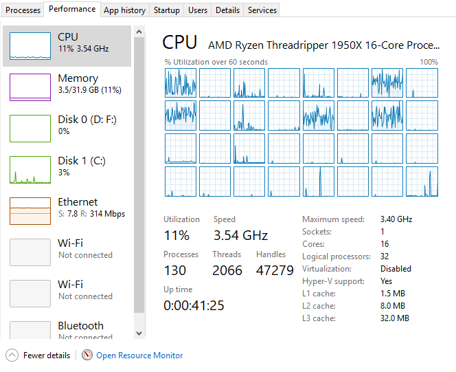
16 cores / 32 threads - helooooow.
The Technology Inside the processor
AMD implemented technology that will make sure that this processor runs applications efficiently and optimized. SenseMI is a set of sensing and adaptive technologies, including an artificial network inside every “Ryzen” series processor to anticipate future decisions, preload instructions, and choose the best path through the CPU. AMD is also introducing a new interconnect called AMD Infinity Fabric. This is a new and fast way of connecting various parts within an SoC. Infinity Fabric is not just used in the the Ryzen generation processors, it is also found in future (Vega) AMD GPUs and (almost) all other AMD chips in the near future. Infinity Fabric allows for faster and better secure connections within a chip. The inter- and intra-chip connector will be standardized and used in many AMD products and, as such, AMD can easily communicate over that very same interconnect. SenseMI technology then; it is based on five parts as shown in the slide below. Pure Power is a technology that allows the Ryzen chips and other Ryzen variants to work as efficiently as possible. Being part of the Ryzen family, Threadripper processors are just that; CPUs based upon Ryzen architecture. While a lot of IO changes have been made to facilitate it the reality is simple: in the processor package you'll spot two 8-core Ryzen processor dies activated, much like the Ryzen 7 1800X has two CCxes with each four cores. This means that Ryzen Threadripper processors have four CCXes. In total that is 2x(2x4) = 16-core procs per processor.
When AMD released Ryzen, all of a sudden there were announcements in their server segment, Naples with up-to a staggering 32 processor cores. And from then onwards, rumors flooded the web. Later in March the first design block diagrams surfaced on the web, indicating that AMD was working on a many-core processor, but one that was to be released to the consumer market, as these diagrams showed an ASUS label. Shortly thereafter the first official announcements were made, AMD would be releasing what we now know to be the X399 chipset platform for motherboards, to be paired with Ryzen Threadripper processors.
You've already seen a number of X399 motherboard announcements, and it is no secret that processors will initially be released in the HEDT (High-End Desktop) segment. Available starting August 10th 2017, AMD will initially release two models: a 16-core, 32-thread model and a 12-core, 24-threaded model, followed shortly by that 8-core SKU offering you quad-channel memory and 64 lanes of PCIe gen 3.0. That memory will run the same clock as the Infinity Fabric. So with the entire platform, you are not making any compromises. But let's talk a little more about the X399 chipset, next page please.
