
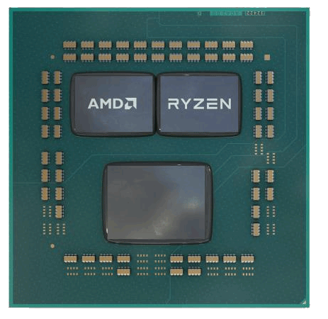
Ryzen 3000 processor family
The Ryzen Generation 3 (Matisse) processors
AMD has been making a series of announcements on their processor platform, several procs, and the new X570 chipset. We’ll first walk through all that new kit to get you an idea of what’s being released and, of course, talk a bit more about the chiplet design and what that is all about. Meet the processors that are going to be injected into the market over the months to follow:
- 16-core Ryzen 9 3950X will be priced 749 USD
- 12-core Ryzen 9 3900XT will be priced 499 USD
- 12-core Ryzen 9 3900X will be priced 499 USD
- 8-core Ryzen 7 3800XT will be priced 399 USD
- 8-core Ryzen 7 3800X will be priced 399 USD
- 8-core Ryzen 7 3700X will be priced 329 USD
- 6-core Ryzen 5 3600XT will be priced 249 USD
- 6-core Ryzen 5 3600X will be priced 249 USD
- 6-core Ryzen 5 3600 will be priced 199 USD
- 4-core Ryzen 3 3300X will be priced 120 USD
- 4-core Ryzen 3 3100 will be priced 99 USD
AMD announced multiple Ryzen 3000 processors with a spread of six to sixteen core products. Ryzen 3600(X) with six cores and twelve threads, 3700(X) (8t/16t), 3800X (8c/16t) And Ryzen 9 3900X (12c/24t). And that means silicon with two 8-core CPU dies immediately enters the market. AMD promises IPC increases of almost 15% and even 25% when you add the increase in clock frequency. Most Ryzen models will get Turbo bins towards 4.4~4.6 GHz. AMD also announced one flagship processor, the Ryzen 9 3950X, a sixteen core part with thirty-two threads and a Turbo binning towards 4.7 GHz.
|
|||||
| CPU | Cores / Threads | Clock speed/turbo (GHz) | Cache (total) | PCIe lanes CPU+x570 chiplet) |
MSRP |
| Ryzen 9 3950X | 16/32 | 3.5 / 4.7 | 72MB | 40 | $ 749 |
| Ryzen 9 3900XT | 12/24 | 3.8 / 4.7 | 70 MB | 40 | $ 499 |
| Ryzen 9 3900X | 12/24 | 3.8 / 4.6 | 70MB | 40 | $ 499 |
| Ryzen 7 3800XT | 8/16 | 3.9 / 4.7 | 36MB | 40 | $ 399 |
| Ryzen 7 3800X | 8/16 | 3.9 / 4.5 | 36MB | 40 | $ 399 |
| Ryzen 7 3700X | 8/16 | 3.6 / 4.4 | 36MB | 40 | $ 329 |
| Ryzen 5 3600XT | 6/12 | 3.8 / 4.7 | 35MB | 40 | $ 249 |
| Ryzen 5 3600X | 6/12 | 3.8 / 4.4 | 35MB | 40 | $ 249 |
| Ryzen 5 3600 | 6/12 | 3.6 / 4.2 | 35MB | 40 | $ 199 |
| Ryzen 3 3300X | 4/8 | 3.8/4.3 | 18MB | 40 | $ 120 |
| Ryzen 3 3100 | 4/8 | 3.6/3.9 | 18MB | 40 | $ 99 |
Chiplet design
AMD is now effectively moving towards a chiplet design starting with Ryzen 3000, aka ZEN2. Multi-die chips, thus multiple chips in one package is what we're talking about when we refer to a chiplet design, it’s one of the many answers to be able to fight off Moore's Law, now and in the future. AMD was already using the technology to connect multiple processors in Threadripper and, for servers, Epyc. Actually, also Intel with Kaby Lake-G. Chiplets, these are multiples of chips put together on an interposer that form the actual chip. Chiplets for AMD Ryzen 3000, Zen 2 feature a I/O die along with 7nm CPU chiplets (each holding eight cores per die). To be able to accomplish that, AMD has been updating its Infinity Fabric that connects the different dies that hold the cores. Current Epyc, Ryzen and Threadripper CPUs are all connected via the Infinity Fabric.
With the Zen 2 architecture, AMD places one I/O die chip that sits in the middle, which is connected to two 8-core dies. These AMD CPU chiplets are connected with 2nd generation Infinity Fabric (the interlink wires that connect them all). Why chiplet designs? One of the bigger issues at hand when manufacturing large monolithic CPU/GPU dies is that yields decrease nearly exponentially, and costs go up due to non-working dies. Multiple smaller chips in one package have higher yields, less loss and thus can be more profitable.
Architecture
Zen 2 architecture is an advancement of Zen, and Zen had some bottlenecks that need to be dealt with. These are solved in this design and, at the same time, thanks to the smaller 7nm transistors, added extra functionality in important places. The image below shows the block diagram of the Zen 2 core. You will spot a new branch predictor, a larger micro-op cache, an additional address generation unit, and a floating point unit, which can handle 256-bits at the same time.
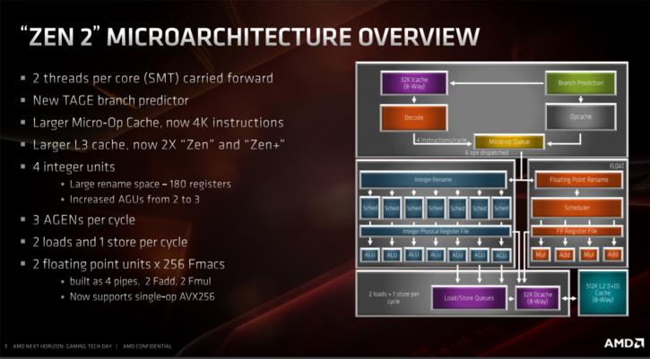
You are going to notice some differences between the three cache levels. The L1 instruction cache has become smaller, the data cache is the same as last gen. The L2 cache is also the same, however, the L3 cache was doubled up from last gen. AMD reduced the L1 instruction cache from 64 kB to 32 kB. The instruction cache contains the x86 instructions that are retrieved from the memory for processing. However, by giving this cache more inputs and outputs, 8-way associative instead of 4-way associative, it will make up for that design choice. Also, by optimizing algorithms for pre-fetching instructions and increasing the caches at other levels (like the L3 cache), the effect of the smaller instruction cache is limited. The L1 data cache was 32 kB in Zen and remains at 32 kB for Zen 2. Also unchanged is the L2 cache, which is still 512 kB per core. The L3 cache, however, is shared by the cores and that one has doubled up in size. Four cores are partitioned together in a group called a core complex (CCX). The earlier generation Zen processors had 8 MB of L3 cache, this has been doubled up to a whopping 16 MB of L3 cache. Why the double L3 cache? Well, AMD needed to address the latencies for accessing working memory to cope with the chiplet design, whereby the memory controller is physically located in a different chip, ergo a doubled L3 cache. Increasing any sort of cache is costly. It takes up a substantial portion of the available transistor budget, here is where 7nm helps out greatly. Ryzen Gen 3 has also been fitted with an improved branch predictor that is now working according to a TAGE algorithm. Scientific studies are indicating that this model predictor offers the best results. Also, an important adjustment is to double the size of the micro-op cache to 4000 instructions. Substantial changes in the new design were also made to the floating point execution units, calculation units that basically do math processing like addition, subtraction, multiplication, division, square root, and bit-shifting. Zen supported 128-bit, Zen 2 makes a move towards 256-bit which brings us to support for AVX2 instructions, these can be processed in one single clock-cycle now. Zen2 does not yet support AVX512. Load/store units have been optimized by doubling bandwidth from 16 bytes per clock cycle to 32 bytes per clock cycle. L/S units transport data to and from the caches and, via that route, to and from the memory.
