
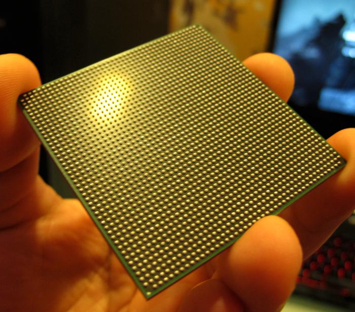
The AMD Fiji GPU
AMD Fiji
So, over the past two years you have been hearing about several codenames and that can be a little confusing. AMD likes to stick to island series GPUs for their codenames, for the Fury series the Fiji GPU gets its denomination from there. AMD Fiji is the new GPU used, we are going to talk about the GPU now and through part of the next page we'll talk a little more in-depth about the HBM that sits on that GPU. But hey, meet Fiji:
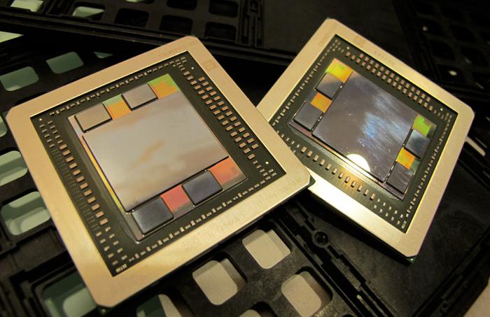
So, at a recent event I was able to snag two Fiji chips. Look at that, the GPU core surrounded by the four stacks of HBM memory.
The Fiji series of GPUs is the next iteration of the GCN (Graphics Core next) architecture. Fiji is based on revision 1.2 GCN, just like Tonga (285 & 380 series). Basically, if we took Tonga and scale that upwards that would be Fiji (but that is an overly generalized explanation).
| AMD Radeon R9 Fury X | AMD Radeon R9 390X | |
| Fabrication Process | 28nm | 28nm |
| GPU | Fiji | Hawaii / Grenada |
| Streaming Processors | 4096 | 2816 |
| Graphics memory | 4 GB HBM | 8 GB GDDR5 |
| Memory Clock | up-to 500 MHz / 1.0 Gbps | 6.0 Gbps |
| Core Clock | 1050 MHz | 1050 MHz |
| Memory Bandwidth | up-to 512 GB/s | 384 GB/s |
| Power Connectors | 2 x 8-pin | 1 x 6-pin - 1 x 8-pin |
| Form Factor | Full Height, Dual slot | Full Height, Dual slot |
| Freesync | Yes | Yes |
| DirectX 12 Support | Yes | Yes |
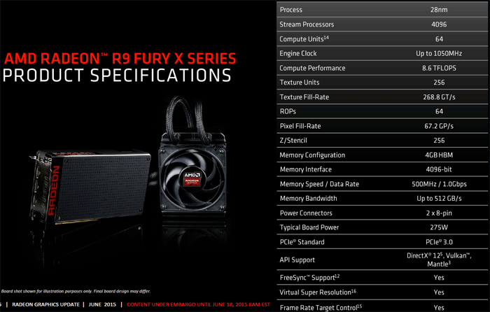
Fiji is still based on a 28nm fabrication node, 20nm failed and until we see 16 and 14nm viable for big GPUs, the 28nm node really is the only alternative. That was the same dilemma for Nvidia with the GTX 980 Ti of course. Both GPUs as a result are big. For Fiji that Mac Daddy is 5x5cm in size. Bigger means higher voltage usage, and thus more heat to deal with. You can only imagine what a chip like this would be like on 14nm, at half the size. AMD did huge things with Fiji though, they tucked away 8.9 Billion transistors on the GPU and that's the number without the memory. It gives them a staggering 8.6 TFLOPS of performance to work with. That, combined with HBM memory, is to be considered serious stuff. The GPU has a whopping amount of transistors. At 28nm AMD applied the GCN 1.2 architecture, albeit you will learn that there have been a few tweaks at cache levels as the L2 cache is now 2MB for example.
| Card | Radeon R9 Fury X | Radeon R9 390X |
| Process | 28nm | 28nm |
| Transistors | 8.9 Billion | 6.2 Billion |
| Engine Clock | 1050 MHz | 1050 MHz |
| Stream Processors | 4,096 | 2,816 |
| Compute Performance | 8.6 TFLOPS | 5.9 TFLOPS |
| Texture Units | 256 | 176 |
| Texture Fillrate | 268.8 GT/s | 176 GT/s |
| ROPs | 64 | 64 |
| Pixel Fillrate | up-to 68.2 Gp/s | up-to 64 Gp/s |
| Z/Stencil | 256 | 256 |
| Memory Bit-Interface | 4096-bit | 512-bit |
| Memory Type | 4GB HBM | 8GB GDDR5 |
| Data Rate | 500 MHz / 1.0 Gbps | 1500 MHz / 6.0 Gbps |
| Memory Bandwidth | 512.0 GB/s | 320.0 GB/s |
| Typical Board Power | 275W | 275W |
| PCI-Express Gen | 3.0 | 3.0 |
| API support | DirectX 12 / Vulkan / Mantle | DirectX 12 / Vulkan / Mantle |
An interesting step from AMD is the move towards a 4096-bit memory bus thanks to HBM. Nobody really expected it as in the past AMD merely placed GDDR on their products. You will notice very similar structures compared to Tonga (Radeon R9 265 and 380). This is GCN 1.2, yet multitudes of it. The Fiji GPU as such has 4096 shader processors, these are clustered up in groups of 64 shader processors per CU (compute unit). 64 units times 64 shaders = 4096.
The 1050 MHz core clock frequency is not a fixed clock on these cards. But in almost all scenarios we have seen it stick precisely at 1050 MHz. But sure, if the card passes its power limitations or overheats then the card would clock up/down in-between these monitored limiters.
