During a keynote speech at our annual GPU Technology Conference in San Jose, Calif., NVIDIA CEO Jen-Hsun Huang updated our public GPU roadmap with the announcement of Pascal, the GPU family that will follow this year’s Maxwell GPUs.
Named for 17th century French mathematician Blaise Pascal, our next-generation family of GPUs will include three key new features: stacked DRAM, unified memory and NVLink.
- 3D Memory: Stacks DRAM chips into dense modules with wide interfaces, and brings them inside the same package as the GPU. This lets GPUs get data from memory more quickly – boosting throughput and efficiency – allowing us to build more compact GPUs that put more power into smaller devices. The result: several times greater bandwidth, more than twice the memory capacity and quadrupled energy efficiency.
- Unified Memory: This will make building applications that take advantage of what both GPUs and CPUs can do quicker and easier by allowing the CPU to access the GPU’s memory, and the GPU to access the CPU’s memory, so developers don’t have to allocate resources between the two.
- NVLink: Today’s computers are constrained by the speed at which data can move between the CPU and GPU. NVLink puts a fatter pipe between the CPU and GPU, allowing data to flow at more than 80GB per second, compared to the 16GB per second available now.
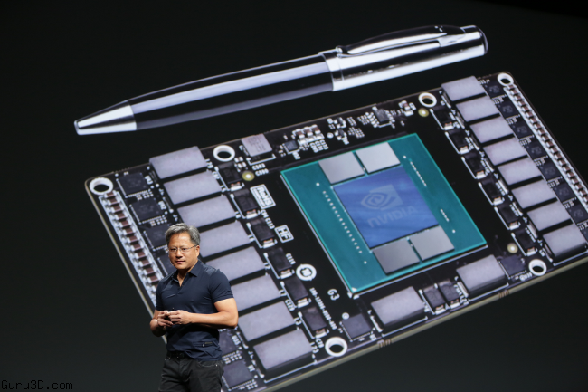
- Pascal Module: NVIDIA has designed a module to house Pascal GPUs with NVLink. At one-third the size of the standard boards used today, they’ll put the power of GPUs into more compact form factors than ever before.
Pascal is due in 2016.
---
NVIDIA GPU accelerators have emerged in High-Performance Computing as an energy-efficient way to provide significant compute capability. The Green500 supercomputer list makes this clear: the top 10 supercomputers on the list feature NVIDIA GPUs. Today at the 2014 GPU Technology Conference, NVIDIA announced a new interconnect called NVLink which enables the next step in harnessing the full potential of the accelerator, and the Pascal GPU architecture with stacked memory, slated for 2016.
Stacked Memory
Pascal will support stacked memory, a technology which enables multiple layers of DRAM components to be integrated vertically on the package along with the GPU. Stacked memory provides several times greater bandwidth, more than twice the capacity, and quadrupled energy efficiency, compared to current off-package GDDR5. Stacked memory lets us combine large, high-bandwidth memory in the same package with the GPU, allowing us to place the place the voltage regulators close to the chip for efficient power delivery. Stacked Memory, combined with a new Pascal module that is one-third the size of current PCIe boards, will enable us to build denser solutions than ever before.
Outpacing PCI Express
Today a typical system has one or more GPUs connected to a CPU using PCI Express. Even at the fastest PCIe 3.0 speeds (8 Giga-transfers per second per lane) and with the widest supported links (16 lanes) the bandwidth provided over this link pales in comparison to the bandwidth available between the CPU and its system memory. In a multi-GPU system, the problem is compounded if a PCIe switch is used. With a switch, the limited PCIe bandwidth to the CPU memory is shared between the GPUs. The resource contention gets even worse when peer-to-peer GPU traffic is factored in.

NVLink addresses this problem by providing a more energy-efficient, high-bandwidth path between the GPU and the CPU at data rates 5 to 12 times that of the current PCIe Gen3. NVLink will provide between 80 and 200 GB/s of bandwidth, allowing the GPU full-bandwidth access to the CPU’s memory system.
A Flexible and Energy-Efficient Interconnect
The basic building block for NVLink is a high-speed, 8-lane, differential, dual simplex bidirectional link. Our Pascal GPUs will support a number of these links, providing configuration flexibility. The links can be ganged together to form a single GPU↔CPU connection or used individually to create a network of GPU↔CPU and GPU↔GPU connections allowing for fast, efficient data sharing between the compute elements.

When connected to a CPU that does not support NVLink, the interconnect can be wholly devoted to peer GPU-to-GPU connections enabling previously unavailable opportunities for GPU clustering.

Moving data takes energy, which is why we are focusing on making NVLink a very energy efficient interconnect. NVLink is more than twice as efficient as a PCIe 3.0 connection, balancing connectivity and energy efficiency.
Understanding the value of the current ecosystem, in an NVLink-enabled system, CPU-initiated transactions such as control and configuration are still directed over a PCIe connection, while any GPU-initiated transactions use NVLink. This allows us to preserve the PCIe programming model while presenting a huge upside in connection bandwidth.
What NVLink and Stacked Memory Mean for Developers
Today, developers devote a lot of effort to optimizing and avoiding PCIe transfer bottlenecks. Current applications that have devoted time to maximizing concurrency of computation and communication will enjoy a boost from the enhanced connection.
NVLink and stacked memory enable acceleration of a whole new class of applications. The large increase in GPU memory size and bandwidth provided by stacked memory will enable GPU applications to access a much larger working set of data at higher bandwidth, improving efficiency and computational throughput, and reducing the frequency of off-GPU transfers. Crafting and optimizing applications that can exploit the massive GPU memory bandwidth as well as the CPU↔GPU and GPU↔GPU bandwidth provided by NVLink will allow you to take the next steps towards exascale computing.
Starting with CUDA 6, Unified Memory simplifies memory management by giving you a single pointer to your data, and automatically migrating pages on access to the processor that needs them. On Pascal GPUs, Unified Memory and NVLink will provide the ultimate combination of simplicity and performance. The full-bandwidth access to the CPU’s memory system enabled by NVLink means that NVIDIA’s GPU can access data in the CPU’s memory at the same rate as the CPU can. With the GPU’s superior streaming ability, the GPU will sometimes be able to stream data out of the CPU’s memory system even faster than the CPU.
NVIDIA Refreshes GPU Roadmap and Announces Pascal