The GV100 GPU
Nvidia Tesla Volta V100 graphics processor
The 815 mm²beast with 5376 shader processors and 21.1 billion transistors
Nvidia announced the Testla Volta V100 processor, this is a Volta based GPU based on Tensor architecture. Tesla Volta V100 will be fabricated on TSMC’s 12nm finfet process, pushing the limits of photo lithography as this GPU is huge. While the Tesla Volta V100 graphics processor has 5120 CUDA / shader processors. But the bigger announcement is that a full GV100 GPU has a total of 5376 cores. In this one page preview a recap of what nvidia announced.
The GV100 Graphics processor
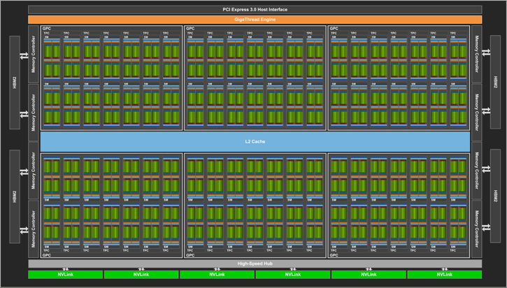
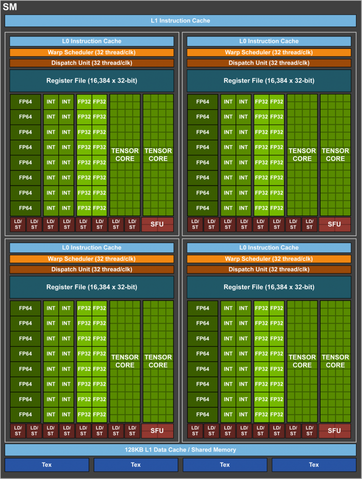
Slightly more detail first as there was some confusion with the Teslta Volta V100 specs and the GV100 GPU used, a fully enabled GV100 GPU actually consists of six GPCs, 84 Volta SMs, 42 TPCs (each including two SMs), and eight 512-bit memory controllers (4096 bits total). Each SM has 64 FP32 Cores, 64 INT32 Cores, 32 FP64 Cores, and 8 new Tensor Cores. Each SM also includes four texture units.
With 84 SMs, a full GV100 GPU thus has a total of 5376 FP32 cores, 5376 INT32 cores, 2688 FP64 cores, 672 Tensor Cores, and 336 texture units. Each memory controller is attached to 768 KB of L2 cache, and each HBM2 DRAM stack is controlled by a pair of memory controllers. The full GV100 GPU includes a total of 6144 KB of L2 cache. The figure in above table shows a full GV100 GPU with 84 SMs (different products can use different configurations of GV100). The Tesla V100 accelerator uses 80 SMs.
A new combined L1 data cache and shared memory subsystem of the Volta SM significantly improves performance while also simplifying programming and reducing the tuning required to attain at or near-peak application performance. Combining data cache and shared memory functionality into a single memory block provides the best overall performance for both types of memory accesses. The combined capacity is 128 KB/SM, more than 7 times larger than the GP100 data cache, and all of it is usable as a cache by programs that do not use shared memory. Texture units also use the cache. For example, if shared memory is configured to 64 KB, texture and load/store operations can use the remaining 64 KB of L1.
The Tesla Volta V100 graphics processor
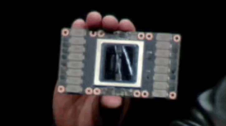
The Tesla Volta V100 graphics processor has 5,120 shader processors active and is based upon an incredible 21 Billion transistors. It offers what Nvidia calls 120 Tensor TeraFLOPS of performance. Gaming wise it would perform in the 15 TFLOP (fp32) region, delivered by a new type of architecture called Tensor cores. The R&D behind this did cost Nvidia many years and about $3 billion worth in investments, CEO JHH stated in his keynote. The first server and deep learning segmented products based on Tesla Volta V100 will become available in Q3 2017. The new Tensor Core is based on a 4×4 matrix array and fully optimized for deep learning. Nvidia stated, they felt Pascal is fast, but isn't fast enough. I already stated that the GPU is huge, it's 815mm2 huge and would fit roughly the palm of your hand.
- Massive 815mm2 die size
- 12nm FinFet (TSMC)
- 21B Transistors
- 15 FP32 TFLOPS / 7.5 FP64 TFLOPS
- 120 Tensor TFLOPS
- 16GB HBM2 which manages @ 900 GB/s
- 5120 Shader processor cores
Tesla Volta V100 is capable of pushing 15 FP32 TFLOPS and much like Pascal GP100 is once again tied towards 4096-bit HBM2 graphics memory (stacked on-die cache). The unit will get 16GB of it divided over four stacks (= 4GB per stack). The memory is fabbed by Samsung. Volta’s 16GB HBM2 memory subsystem delivers 900 GB/sec peak memory bandwidth. This is 1.5x delivered memory bandwidth versus Pascal GP100. Tesla V100 delivers industry-leading floating-point and integer performance. Peak computation rates (based on GPU Boost clock rate) are:
- 7.5 TFLOP/s of double precision floating-point (FP64) performance;
- 15 TFLOP/s of single precision (FP32) performance;
- 120 Tensor TFLOP/s of mixed-precision matrix-multiply-and-accumulate.
That HUGE die at 815 mm2 is fabbed by TSMC on a 12nm FFN fabrication process. In Q3 you will see the first enterprise based products based on Volta that start at 69.000 dollar. For us gamers, when GeForce GTX 1180 or 2080 will be released. That remains to be topic of a long discussion. Below a comparative specification list of the primary Tesla GPUs running up-to Volta, which runs in the 5120 shader processors at the 1.45 GHz marker for Boost frequency btw. It'll have 320 Texture Units, sheesh.