2 - Anatomy of the Chipset
Anatomy of the chipset
To understand what exactly the GeForce 9800 GX2 is we must first go back to the two GPU cores this product has embedded. Therefore first a quick chat about the graphics processors developed under the name "G92".
If you think you recognize that codename, you are onto something. The name G92, is the GPU used in the product you better know as GeForce 8800 GTS, specifically the 512MB models. That product alone comes close, performance wise, to the GeForce 8800 GTX, so imagine what two of them combined can do in terms of performance.
The G92 silicon is based on NVIDIA's newer 0.65nm silicon. Much like the 8800 GT? Is this a respin chip? Rhetorical questions answered "Yes and no, but not exactly". See while this GPU architecture is 95% the same as the good old G80 (GTS/GTX/Ultra) core there are some very distinct differences
The first being the fabrication process. It was moved from 90nm towards 65nm, meaning a smaller die-size, likely resulting in lower core voltages, better energy efficiency and perhaps better clock speeds. The second positive here is that the product has an increased amount of shader processors over the precious GTS 320/640MB series (while being a cheaper chip to make). Let me explain: a 8800 GTX has 128 of these Shader processors embedded onto the graphics core, the old model 8800 GTS (320/640MB) has 96 shader processors, the new 8800 GT has 112 activated Shader processors, yet importantly the G92 is based on the 8800 GTS 512MB which means that both GPUs on the 9800 GX2 have 128 shader processors.
Interesting, because if you take a peek at the clock speeds you'd might even think that one G92 GPU could beat a GTX. Well shader processors are not the only part of the equation, because at the end of the pipeline there this thing called ROPs, and that's where the old GTS (20 ROPs), and this G92 (16 ROPs) become a little castrated compared to the GTX (24 ROPs). There's a new optimization of ROPs' compression algorithm being applied on the GT though, which makes it a bit more efficient.
Next to that, the G92 is utilizing more memory than the GTX, yet the GTX is addressing the memory bus faster (384-bit) as opposed to the G92 with 256-bit, that's less memory bandwidth to play around with.
The performance differential between the two processors is small though, as our benchmarks have shows on the 8800 GTS articles.
A logical question on your end would be, why is the 9800 GX2 a series 9 product, and the 8800 GTS 512MB based on the same G92 graphics core, a Series 8 product?
My answer; I have no idea other than the fact that a Series 9 product sounds better (marketing wise). The G92 based 8800 GTS should probably have been called 9800 GTS or GS as people in the stores right now are really confused.
So in summary, the new features of G92 opposed to the G80, smaller 65nm fabrication process, silicon optimizations (compression algorithms), usage of 256-bit memory and compared to the older GTS models, a high shader processor count at 128 sub-cores.
But then NVIDIA launched the GeForce 9800 GX2 ... which has two of these graphics processors embedded into one product.
The reference 9800 GX2
Since we covered the basics of the G92 processor we can now talk a bit about the actual GX2 itself. It's the year 2008, you guys are familiar with abbreviations like SLI and Crossfire. In a very short layman explanation, this is the technology that NVIDIA is applying at the 9800 GX2, it's a very fast and relatively cheap to develop method to produce a fast performing product.
There are however some deficits, but we'll discuss them later on in this chapter. See basically what NVIDIA did is to take two 8800 GTS 512MB graphics cards, merged them together and made sure it's working as a "single" functional graphics card. Why do I say that so specifically ? Because typically with SLI you are forced to use a nForce mainboard series where with a GX2 you can use the product in for example an Intel mainboard just as well. So when you open of the casing of that huge looking graphics card, you'd notice two PCBs, two GPUs, and two sets of 512MB memory. Yes, everything is doubled up yet bound to one big cooler sitting in the middle between the two GPUs.
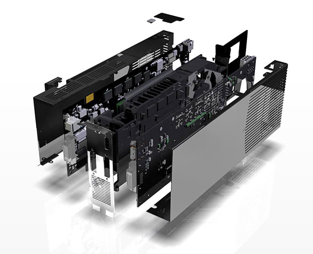
Two PCBs, two set's of memory, one PCB flipped around so one cooler is used. Engineering wise, this is art.
Let's get a misconception out of the way first though. Loads of manufacturers had the nerve to label this product have a 512-bit memory bus. This is not true, the memory connected to the G92 is running 100% over the 256-bit wide controller. But since everything is doubled up (two set's of memory and thus two controllers) some board-partners would "love" to make you believe it's 512-bit.
Now there's no shame in 256-bit people, if anything the Radeon cards with 512-bit memory controller and memory proved that 512-bit is not quite yet the answer. It's a lot more wires in that PCB, very complex and it's very hard to see a real gain in performance. Alright, so remember .. 256-bit.
Two GPU's create a lot of heat and consume a lot of power. This might be the reason that the core frequency of the 9800 GX2 GPUs are clocked slower than the G92 on the 8800 GTS 512MB. It beats me, but for the referece product the core is running at 600 MHz, the Shaders processors at 1500 MHz and memory at a beefy 2000 MHz.
Initially NVIDIA did not allow overclocked products to be released, but that has changed. It's also were we end up with today's tested product. Next chapter.
