Architecture Deep Dive
Architecture Deep Dive
For the real gurus, allow me to sidetrack a minute and go a little deeper into the architecture of the GPU, the design block. For those wondering, NVIDIA is moving to a MIMD layout as they feel it will work out better for them with stream computing (GPGPU), ATI however is using a SIMD layout. There are 20 SIMD clusters each with 16 thread processors. Each thread processor has 5 stream cores (and that makes 1600 shader cores). Since there are 80 texture units the card will have four per SIMD cluster available.
Each shader (thread) processor has:
- Four stream cores plus one special function stream
- Branch unit
- General purpose registers
When we move onwards to texture units and caches we notice some improvements as well. There's an increased texture bandwidth (up to 68 billion bilinear filtered texels/sec with up-to 272 billion 32-bit fetches/sec. But let's have a look at the GPU design with the help of a block diagram:
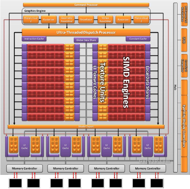
So this is how the GPU is arranged. Cache wise the GPU of course has embedded L1 and L2 caches. We know that the L1 cache can now handle texture fetches up to 1 TB/sec on the L1 cache and 435 GB/sec in-between L1 and L2. Each memory controller has 128 kB L2 cache.
Hardware wise the architecture had to change somewhat for new DX11 features. 90% of the design remained the same but obviously with DX11 also comes hardware tessellation. As such, in the ASIC next to dual rasterizers we now spot a new DX11 class hardware tessellation unit (we'll explain what tessellation is later). The tessellation unit will be programmable through DX11 hull and domain shaders and is a feature I'm really excited about.
 On the topic of image quality, texture filtering has been improved as well, imposing an even better quality Anisotropic filtering. Anisotropic filtering no longer has angle dependency. You'll now have near perfect Anisotropic filtering, look at the image to the right. I understand that screenshots does not make a lot of sense to a lot of you, but really .. this is what we want to see, that's a near perfect filter.
Memory wise the card will use 256-bit DDR5 memory again. It's clocked faster though, adding additional bandwidth. Memory bandwidth is so important.
Thanks to some changes in the memory controllers relativity has gone up, as well as energy efficiency. Especially with DX Compute where crunching data is so important and needs to be reliable, we now see a new feature; error detection code is now embedded in the GDDR5 memory controller.
Some of the new memory controller improvements:
- EDC - error detection code (CRC checks on data transfers)
- GDDR5 Memory Clock Temperature compensation
- Fast GDDR5 Link retraining (allows voltage and clock switching without any problems or hassle)
But yes, EDC is the most important one here as it improves reliability at very high clock frequencies.
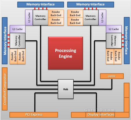 block diagram of the memory controller setup
Voltage regulation
Good news for the die-hard overclockers. This card will be softmod compatible as it has programmable voltage regulators which allow you to in/decrease voltages on the GPU. VRM implementation is impressive, obviously it allows ATI to lower voltages when needed, saving on power consumption. Overclockers think the other way arround ;)
Four digital vGPU phases controlled with the Volterra VT1157SF, one digital uncore (GDDR5 IMC) phase with Volterra VT1157SF, 1+1 "digital" GDDR5 vDD+vDDQ phases with Volterra VT242WF, two Volterra VT1165MF controllers (vGPU & uncore).
The PCB surely shows a very impressive VRM design.
