Pascal GPU Architecture
The Pascal GP102-350 GPU
The GPU is based on DX12 compatible architecture called Pascal. Much like in the past designs you will see pre-modelled SMX clusters that hold what is 2x64 shader processors per cluster. Pascal GPUs are composed of different configurations of Graphics Processing Clusters (GPCs), Streaming Multiprocessors (SMs), and memory controllers. Each SM is paired with a PolyMorph Engine that handles vertex fetch, tessellation, viewport transformation, vertex attribute setup, and perspective correction. The GP102 PolyMorph Engine also includes a new Simultaneous Multi-Projection units. There are 28 active (SM) clusters for a fully enabled Pascal GP102 GPU. The NVIDIA GeForce GTX 1080 Ti however is not fully enabled. Thus two out of two GPCs have been disabled.
- The GeForce GTX 1060 (GP104-400) has 10 x 128 shader processors makes a total of 1,280 shader processors.
- The GeForce GTX 1070 (GP104-200) has 15 x 128 shader processors makes a total of 1,920 shader processors.
- The GeForce GTX 1080 (GP104-400) has 20 x 128 shader processors makes a total of 2,560 shader processors.
- The GeForce GTX 1080 Ti (GP102-350) has 28 x 128 shader processors makes a total of 3,584 shader processors.
- The Nvidia Titan X (GP102-400) has 28 x 128 shader processors makes a total of 3,584 shader processors.
Each SM has a cluster of 64 shader / stream / cuda processors doubled up. Don't let that confuse you, it is 128 shader units per SM. Each GPC ships with a dedicated raster engine and 28 SMs. Each SM contains 128 CUDA cores, 256 KB of register file capacity, a 96 KB shared memory unit, 48 KB of total L1 cache storage, and eight texture units. The 1080 Ti card will be released with a core clock frequency of 1.48 GHz with a Boost frequency that can run up to 1.58 GHz (and even higher depending on load and thermals).
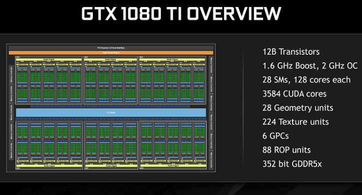
As far as the memory specs of the GP102 GPU are concerned, these boards will feature a 352-bit memory bus connected to a nice 11 GB of GDDR5X video memory, AKA VRAM AKA framebuffer AKA graphics memory for the graphics card. The GeForce GTX 1000 series are DirectX 12 ready, in our testing we'll address some Async compute tests as well as Pascal now has Enhanced Async compute. The latest revision of DX12 is a Windows 10 feature only, yet will bring in significant optimizations. With 11 GB graphics memory available for one GPU, the card is very attractive for both modern and future games no matter what resolution you game at.
Color Compression
The card uses GDDR5X memory, the really good stuff at 11,000 MHz (effective), 11 GB and all on a 352-bit wise memory bus. Well, you can never have too much bandwidth so Nvidia applied some more tricks, color compression being one of them. The GPU’s compression pipeline has a number of different algorithms that intelligently determine the most efficient way to compress the data. One of the most important algorithms is delta color compression. With delta color compression, the GPU calculates the differences between pixels in a block and stores the block as a set of reference pixels plus the delta values from the reference. If the deltas are small then only a few bits per pixel are needed. If the packed together result of reference values plus delta values is less than half the uncompressed storage size, then delta color compression succeeds and the data is stored at half size (2:1 compression). Pascal GPUs include a significantly enhanced delta color compression capability:
- 2:1 compression has been enhanced to be effective more often
- A new 4:1 delta color compression mode has been added to cover cases where the per pixel deltas are very small and are possible to pack into ¼ of the original storage
- A new 8:1 delta color compression mode combines 4:1 constant color compression of 2x2 pixel blocks with 2:1 compression of the deltas between those blocks
With that additional memory bandwidth combined with new advancements in color compression Nvidia can claim even more bandwidth as Pascal cards now use 4th generation delta color compression thanks to enhanced color compression and enhanced caching techniques. Up-to Maxwell the GPU could handle 2:1 color compression ratios, newly added are 4:1 and 8:1 delta color compression. So on one hand the Raw memory bandwidth increases 1.4x~1.5x (for the GeForce GTX 1080 / Ti / Titan X with GDDR5X) and then there's a compression benefit of 1.2x for the GeForce GTX 1000 series which is a nice step up in this generation technology wise. Overall there is an increase of roughly 1.7x in memory bandwidth thanks to the faster memory and new color compression technologies. More effective bandwidth thanks to enhanced color compression and enhanced caching techniques. The effectiveness of delta color compression depends on the specifics of which pixel ordering is chosen for the delta color calculation. The GPU is able to significantly reduce the number of bytes that have to be fetched from memory per frame.
Pascal Graphics Architecture
Let's place the more important data on the GPU into a chart to get an idea and better overview of changes in terms of architecture like shaders, ROPs and where we are at frequencies wise:
 | ||||||
|---|---|---|---|---|---|---|
| Reference GeForce | GTX 1080 Ti | Titan X | GTX 1080 | GTX 1070 | GTX 1060 | GTX 980 Ti |
| (2016 edition) | ||||||
| GPU | GP102-350-A1 | GP102-400-A1 | GP104-400-A1 | GP104-200-A1 | GP106-400-A1 | GM200 |
| Architecture | Pascal | Pascal | Pascal | Pascal | Pascal | Maxwell |
| Transistor count | 12 Billion | 12 Billion | 7.2 Billion | 7.2 Billion | 4.4 Billion | 8 Billion |
| Fabrication Node | TSMC 16 nm | TSMC 16 nm | TSMC 16 nm | TSMC 16 nm | TSMC 16 nm | TSMC 28 nm |
| CUDA Cores | 3,584 | 3,584 | 2,560 | 1,920 | 1,280 | 2,816 |
| SMMs / SMXs | 28 | 28 | 20 | 15 | 10 | 22 |
| ROPs | 88 | 96 | 64 | 64 | 48 | 96 |
| GPU Clock Core | 1,480 | 1,417 MHz | 1,607 MHz | 1,506 MHz | 1,506 MHz | 1,002 MHz |
| GPU Boost clock | 1,582 | 1,531 MHz | 1,733 MHz | 1,683 MHz | 1,709 MHz | 1,076 MHz |
| Memory Clock | 2752 MHz | 2500 MHz | 1,250 MHz | 2,000 MHz | 2,000 MHz | 1,753 MHz |
| Memory Size | 11 GB | 12 GB | 8 GB | 8 GB | 3 GB / 6 GB | 6 GB |
| Memory Bus | 352-bit | 384-bit | 256-bit | 256-bit | 192-bit | 384-bit |
| Memory Bandwidth | 484 GB/s | 480 GB/s | 320 GB/s | 256 GB/s | 192 GB/s | 337 GB/s |
| FP Performance | 11.5 TFLOPS | 11.0 TFLOPS | 9.0 TFLOPS | 6.45 TFLOPS | 4.61 TFLOPS | 6.4 TFLOPS |
| GPU Thermal Threshold | 91 Degrees C | 91 Degrees C | 94 Degrees C | 94 Degrees C | 94 Degrees C | 91 Degrees C |
| TDP | 250 Watts | 250 Watts | 180 Watts | 150 Watts | 120 Watts | 250 Watts |
| Launch MSRP ref | $699 | $1200 | $599 | $379/$449 | $249/$299 | $699 |
So we talked about the core clocks, specifications and memory partitions. However, to be able to better understand a graphics processor you simply need to break it down into tiny pieces. Let's first look at the raw data that most of you can understand and grasp. This bit will be about the architecture. NVIDIA’s “Pascal” GPU architecture implements a number of architectural enhancements designed to extract even more performance and more power efficiency per watt consumed. Above, in the chart photo, we see the block diagram that visualizes the architecture, Nvidia started developing the Pascal architecture around 2013/2014 already. The GPCs have 28 SMX/SMM (streaming multi-processors) clusters in total. You'll spot twelve 32-bit memory interfaces, bringing in a 384-bit path to the graphics GDDR5X memory pipeline. Tied to each 32-bit memory controller are eight ROP units and 256 KB of L2 cache. Simple math now tells us the full GP102 chip used in Titan X thus has a total of 96 ROPs and 3,072 KB of L2 cache. What about double-precision? It's dumbed down to not interfere with Quadro sales -- double-precision instruction throughput is 1/32 the rate of single-precision instruction throughput. So the compute capabilities are:
- FP32 : 11TF, INT8 : 44TOPS
- FP64 : 11TF x 1/32
- FP16 : 11TF x 1/64 (but can use lib to convert FP16 to FP32)
An important thing to focus on is the SM (block of shader processors) clusters (SMX), which have 128 shader processors. One SMX holds 128 single‐precision shader cores, double‐precision units, special function units (SFU), and load/store units. So based on a full 28 SM (3.584 shader proc) core chip the looks are fairly familiar in design. In the pipeline we run into the ROP (Raster Operation) engine and the GP102 has 96 engines for features like pixel blending and AA. The GPU has 64 KB of L1 cache for each SMX plus a special 48 KB texture unit memory that can be utilized as a read-only cache. The GPU’s texture units are a valuable resource for compute programs with a need to sample or filter image data. The texture throughput then, each SMX unit contains 8 texture filtering units.
- GeForce GTX 960 has 8 SMX x 8 Texture units = 64
- GeForce GTX 970 has 13 SMX x 8 Texture units = 104
- GeForce GTX 980 has 16 SMX x 8 Texture units = 128
- GeForce Titan X has 24 SMX x 8 Texture units = 192
- GeForce GTX 1060 has 10 SMX x 8 Texture units = 80
- GeForce GTX 1070 has 15 SMX x 8 Texture units = 120
- GeForce GTX 1080 has 20 SMX x 8 Texture units = 160
- NVIDIA GTX 1080 Ti has 28 SMX x 8 Texture units = 224
- NVIDIA Titan X (2016) has 28 SMX x 8 Texture units = 224
So there's a total of up-to 28 SMX x 8 TU = 224 texture filtering units available for the silicon itself. Actually 240 if all SMXes would have been enabled for the SKU.
Asynchronous Compute
Modern gaming workloads are increasingly complex, with multiple independent, or “asynchronous,” workloads that ultimately work together to contribute to the final rendered image. Some examples of asynchronous compute workloads include:
- GPU-based physics and audio processing
- Postprocessing of rendered frames
- Asynchronous timewarp, a technique used in VR to regenerate a final frame based on head position just before display scanout, interrupting the rendering of the next frame to do so
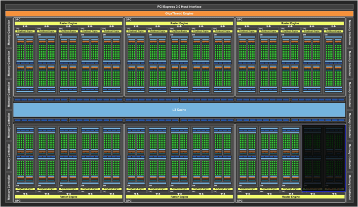
These asynchronous workloads create two new scenarios for the GPU architecture to consider. The first scenario involves overlapping workloads. Certain types of workloads do not fill the GPU completely by themselves. In these cases there is a performance opportunity to run two workloads at the same time, sharing the GPU and running more efficiently — for example a PhysX workload running concurrently with graphics rendering. For overlapping workloads, Pascal introduces support for “dynamic load balancing.” In Maxwell generation GPUs, overlapping workloads were implemented with static partitioning of the GPU into a subset that runs graphics, and a subset that runs compute. This is efficient provided that the balance of work between the two loads roughly matches the partitioning ratio. However, if the compute workload takes longer than the graphics workload, and both need to complete before new work can be done, and the portion of the GPU configured to run graphics will go idle. This can cause reduced performance that may exceed any performance benefit that would have been provided from running the workloads overlapped. Hardware dynamic load balancing addresses this issue by allowing either workload to fill the rest of the machine if idle resources are available.
Time critical workloads are the second important asynchronous compute scenario. For example, an asynchronous timewarp operation must complete before scanout starts or a frame will be dropped. In this scenario, the GPU needs to support very fast and low latency preemption to move the less critical workload off of the GPU so that the more critical workload can run as soon as possible. As a single rendering command from a game engine can potentially contain hundreds of draw calls, with each draw call containing hundreds of triangles, and each triangle containing hundreds of pixels that have to be shaded and rendered. A traditional GPU implementation that implements preemption at a high level in the graphics pipeline would have to complete all of this work before switching tasks, resulting in a potentially very long delay. To address this issue, Pascal is the first GPU architecture to implement Pixel Level Preemption. The graphics units of Pascal have been enhanced to keep track of their intermediate progress on rendering work, so that when preemption is requested, they can stop where they are, save off context information about where to start up again later, and preempt quickly. The illustration below shows a preemption request being executed.
In the command pushbuffer, three draw calls have been executed, one is in process and two are waiting. The current draw call has six triangles, three have been processed, one is being rasterized and two are waiting. The triangle being rasterized is about halfway through. When a preemption request is received, the rasterizer, triangle shading and command pushbuffer processor will all stop and save off their current position. Pixels that have already been rasterized will finish pixel shading and then the GPU is ready to take on the new high priority workload. The entire process of switching to a new workload can complete in less than 100 microseconds (μs) after the pixel shading work is finished. Pascal also has enhanced preemption support for compute workloads. Thread Level Preemption for compute operates similarly to Pixel Level Preemption for graphics. Compute workloads are composed of multiple grids of thread blocks, each grid containing many threads. When a preemption request is received, the threads that are currently running on the SMs are completed. Other units save their current position to be ready to pick up where they left off later, and then the GPU is ready to switch tasks. The entire process of switching tasks can complete in less than 100 μs after the currently running threads finish. For gaming workloads, the combination of pixel level graphics preemption and thread level compute preemption gives Pascal the ability to switch workloads extremely quickly with minimal preemption overhead.
