The GeForce GTX 480 graphics processor
The GeForce GTX 480 graphics processor
Alright, let's get this article started, as always we'll have a look at Geforce GTX 480 reference specifications first.
NVIDIA released two high-end class DirectX 11 capable products and, as of recently, two mid-range DirectX 11 class products. Firstly, all the new graphics adapters are of course DirectX 11 ready. With Windows 7 and Vista also being DX11 ready all we need are some games to take advantage of DirectCompute, multi-threading, Hardware Tessellation and new shader 5.0 extensions. DX11 is going to be good and once tessellation kicks into games, much better looking.
- GeForce GTX 480 : 480 SP, 384-bit, 250W TDP
- GeForce GTX 470 : 448 SP, 320-bit, 225W TDP
Some of you will say "huh?" as everybody expected 512 shader processors on the top of the line model, 272 cores more than the GT200 (GeForce GTX 280/285). We were as surprised as you guys when we learned that it turned out to be 480 shader processors for the GeForce GTX 480. See, the Fermi architecture, the GF100 graphics processor has sixteen shader clusters embedded in it (called SMs). For the GeForce GTX 480 one such a cluster is disabled, and on the GeForce GTX 470 (though expected) two are disabled.
As to why one SM is disabled on the GeForce GTX 480, we can only speculate. But we have reason to believe that NVIDIA did this to secure better yields and ramp volume production up. Also, much like the GeForce GTX 260 SP216, for the future to be able to introduce a slightly faster SKU with the full 512 SPs. The reality remains that it will not matter 'heaps' in terms of performance as you lose only one-sixteenth of shader performance.
The GeForce GTX 400 cards have the Fermi family chip embedded on them. That chip is called GF100. The GF100 GPU is placed onto an 8-layer PCB and tied to gDDR5 memory. On the topic of graphics memory; NVIDIA made their memory controller GDDR5 compatible, which was not the case on GT200 based GeForce GTX 260/275/285/295, hence their GDDR3 memory.
Memory wise expect large, exemplary large numbers, as we are passing 1 GB. Each utilized memory controller on the respective GPU will get 256MB of memory tied to it.
- The GTX 470 has five memory controllers (5x256MB) = 1280 MB of GDDR5 memory
- The GTX 480 has six memory controllers (6x256MB) = 1536 MB of GDDR5 memory
As you can understand, the massive memory partitions, bus-width and combination of GDDR5 memory (quad data rate) allow the GPU to work with a very high framebuffer bandwidth. So we had a chat about the GF100 GPU and memory. It's now time to break down the GPU clocks:
| GeForce 9800 GTX |
GeForce GTX 285 |
GeForce GTX 295 |
GeForce GTX 470 |
GeForce GTX 480 | |
| Stream (Shader) Processors | 128 | 240 | 240 x2 | 448 | 480 |
| Core Clock (MHz) | 675 | 648 | 576 | 607 | 700 |
| Shader Clock (MHz) | 1675 | 1476 | 1242 | 1215 | 1400 |
| Memory Clock (effective MHz) | 2200 | 2400 | 2000 | 3350 | 3700 |
| Memory amount | 512 MB | 1024 MB | 1792 MB | 1280 | 1536 |
| Memory Interface | 256-bit | 512-bit | 448-bit x2 | 320-bit | 384-bit |
| Memory Type | gDDR2 | gDDR3 | gDDR3 | gDDR5 | gDDR5 |
| HDCP | Yes | Yes | Yes | Yes | Yes |
| Two Dual link DVI | Yes | Yes | Yes | Yes | Yes |
| HDMI | No | No | No | Yes | Yes |
The MSI GeForce GTX 480 Lightning
So the GeForce GTX 480 has a big fat memory partition alright, 1,54 GB of GDDR5 memory which is tied to a 384-bit memory bus that binds to six memory controllers inside the GPU; six memory controllers x 64-bit = 384-bit. This memory is clocked at 950 MHz (= 3800 MHz effective).
Core frequencies then. The MSI GeForce GTX 480 lightning will have its core clocked at 750 MHz, coming from 700 MHz reference. Its shader processors at 1500 MHz.
| Graphics card | GeForce GTX 470 | GeForce GTX 480 | MSI GTX 480 Lightning |
| Fabrication node | 40nm | 40nm | 40nm |
| Shader processors | 448 | 480 | 480 |
| Streaming Multiprocessors (SM) | 14 | 15 | 15 |
| Texture Units | 56 | 60 | 60 |
| ROP units | 40 | 48 | 48 |
| Graphics Clock (Core) | 607 MHz | 700 MHz | 750 MHz |
| Shader Processor Clock | 1215 MHz | 1401 MHz | 1500 MHz |
| Memory Clock / Data rate | 837 MHz / 3348 MHz | 924 MHz / 3696 MHz | 1000 MHz / 4000 MHz |
| Graphics memory | 1280 MB | 1536 MB | 1536 MB |
| Memory interface | 320-bit | 384-bit | 384-bit |
| Memory bandwidth | 134 GB/s | 177 GB/s | 192 GB/s |
| Power connectors | 2x6-pin PEG | 1x6-pin PEG, 1x8-pin PEG | 1x6-pin PEG, 1x8-pin PEG |
| Max board power (TDP) | 215 Watts | 250 Watts | 275 Watts |
| Recommended Power supply | 550 Watts | 600 Watts | 600 Watts |
| GPU Thermal Threshold | 105 degrees C | 105 degrees C | 105 degrees C |
So we talked about the core clocks, specifications and memory partitions. Obviously there's a lot more to talk through. Again, for an in-depth explanation of the GF100 architecture please visit this article we wrote earlier this year.
Now, at the end of the pipeline we run into an improved ROP (Raster Operation) engine, and the GTX 480 has 48 units for features like pixel blending and AA. There's a total of 60 texture filtering units available for the GTX 480. The math is simple here, each SM has four texture units tied to it.
- GeForce GTX 470 has 14 SMs X 4 Texture units = 56
- GeForce GTX 480 has 15 SMs X 4 Texture units = 60
- A fictional GeForce GTX 485 would have 16 SMs x4 TUs = 64
What's also interesting about the GTX 400 release, but was a challenge, is the move towards a smaller die and fabrication process (40nm) which often brings several advantages. One advantage is that you can insert more transistors into the silicon; as such the GF100 GPU comes with 3 billion transistors embedded into it.
Despite a smaller die however, TDPs are relatively high, the GTX 480 will consume at maximum 250 Watts. The KFA2 card however comes factory overclocked, add another 25W.
TDP = Thermal Design Power - roughly translated, when you stress everything on the graphics card 100% of your maximum power consumption is the TDP.
The GeForce GTX 480 comes with both a 6-pin and 8-pin power connector to get enough current and a little spare for overclocking. This boils down as: 8-pin PEG = 150W + 6-pin PEG = 75W + PCIe slot = 75W is 300W available (in theory).
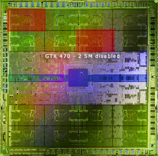
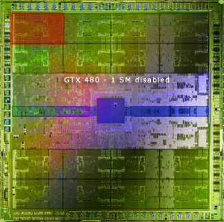 Graphics processor die photo's displaying the number of SMs, the GF100 still has one SM left
