The APU for the A85X FCH
The APU for the A85X FCH
As you guys have learned by now an APU is a processor series with integrated graphics (in the processor die), an idea much like what Intel did with Sandy Bridge and later on Ivy Bridge processors.
APU is an abbreviation of an Accelerated Processing Unit. Back in 2005, when AMD bought ATI, rumors immediately popped up about the technology you will learn about today. Earlier in 2011 you have noticed the introduction of APUs like the E350 (Zacate and Ontario chips), these however can be seen as 'Atom' like processors for netbooks and entry level notebooks. The Llano series was intended to address the entry-level to mid-range segment of both the notebook, but also desktop market.
The APU processor reviewed today for example is targeted against Intel's Sandy Bridge Core i5 2300 processors. Now, processor power wise things will be easy, Intel has the upper hand, but the GPU architecture in Trinity is just so much more advanced allowing you to do much more with less components in your PC, especially in the multi-media segment. Llano APUs are going to dominate as that overall experience is much more powerful.
Combine that with a much more advanced motherboard chipset and the new A85 series motherboards, and you'll notice that AMD has a lot more to bring to the table.
Trinity as a package
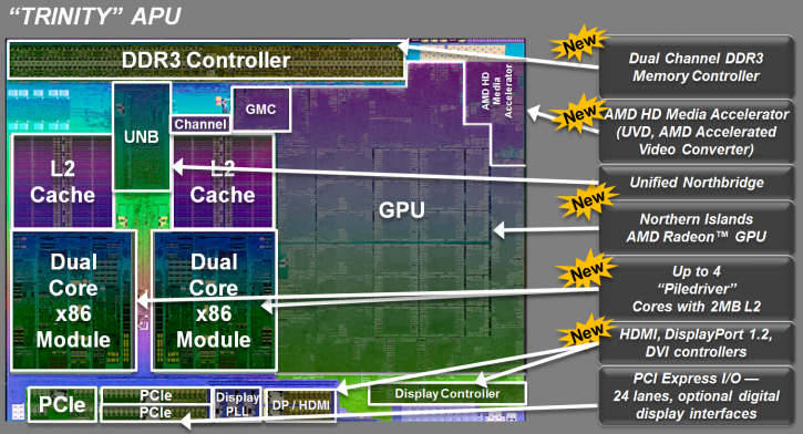
As explained in the introduction AMD is now applying Trinity technology towards the new APUs. The last generation technology was called Llano, which will remain available for quite a while we think. Trinity is based on the very same 32nm fabrication but the chip is completely new. For the CPU part this APU now comes with what is called piledriver cores, four of them. The Piledriver core is the 2nd generation Bulldozer core which on that end you guys all know from the FX series processors.
For the GPU part of the APU things have changed massively. Trinity has a Radeon GPU with 384 shader cores (less are activated depending on SKU). The distict difference is that Llano had an architecture based on the Radeon 5000, Trinity makes use of Radeon 6000 architecture which you all know under the northern islands codenames. Also an upgraded model video-encoder has been integrated, based on the latest Radeon 7000 series.
- AMD calls the GPU embedded into the A10 5800K the Radeon HD 7660D, it runs at 800 MHz.
- AMD calls the GPU embedded into the A8 5600K the Radeon HD 7560D, it runs at 760 MHz.
Trinity comes with a dual-channel memory controller with official support up-to 1866 MHz, new is low voltage memory support which will make the use of 1.25V and 1.5V very easy. Just like Llano Trinity makes use of an integrated PCI_Express 2.0 controller which you can use for a dedicated graphics card. In fact we'll try that out with a GeForce GTX 580 later on in the article. There are 25 PCIe lanes available of which four are used for the chipset
Trinity will have a slightly higher die-size opposed to the previous generation at 246 mm²with 1.3 Billion transistors. To make a bold comparison, Intel has a 216mm² die on 32nm Sandy bridge processors which have 1.16 Billion transistors. Ivy bridge his 160mm² (22nm) with 1.4 Billion transistors.
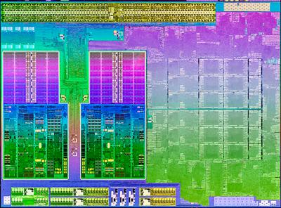
Trinity APU die
Trinity Piledriver CPU Cores
We do need to get a littler deeper into the processors cores as thee have been significant changes. The 2nd generation Bulldozer cores are Piledriver, as such Piledriver cores are used inside the new Trinity APUs. Honestly we have not been very positive about Bulldozer at all as the performance per core simply is not up-to snuff anno 2012.
AMD claims that they have tweaked the logical CPU cores a little to make them perform the way they are intended to be. Inside the APu you'll spot two clusters, or modules fir the CPU side of things. Inside the modules we see two integer CPU-cores which both share a floating point unit. Each module has a 2MB L2 cache. Trinity uses two of these modules which brings it towards four logical processor cores.
Mind you that there will be Trinity versions out with one module disabled, and thus will be 2-core solutions.
That also means that each of the four CPU cores will have 64KB instruction + 64KB data L1 cache per CPU core. Then there's 1MB of L2 cache per CPU core and for Piledriver. There's no shared L3 cache. The processor cores have been tweaked though the average instruction per clock-cycle has improved by a another say 10%
Good news is to see support for AVX, AVX 1.1, FMA3 and AES instructions sets, something Llano missed out on.
One more improvement for Trinity is AMD Turbo Core 3.0, and the technology has been enhanced. The Turbo mode can clock the processor cores up and down real fast when the power usage and temperature allow for it. The A10-5800K APU tested today can turbo towards 4200 MHz.
So Trinity has three primary elements merged into the APU; the Northbridge, the CPU and the GPU. Intel places more focus on raw CPU performance, AMD places more focus on the multi-media experience, thus the GPU.
There's a heck of a lot more to be found inside the APU though, a DDR3 memory controller, Unified Video Decoder core logic, that Northbridge, a PCI Express interface (24 lanes) and of course a DDI interface to output to digital monitors.