The product architecture
The product architecture
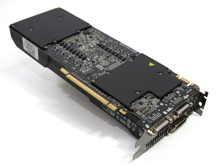
It isn't exactly a secret anymore what the GTX 590 exactly is, in very few words it is one graphics card made out of two graphics processors. Internally they are connected through a PCIe connection (on board) and then they operate in SLI mode. To accomplish something really sturdy and powerful, NVIDIA took their fastest GPUs available and without any compromises on the number of shader processors etc. inside that GPU they started designing the card.
The end result is a dual-GPU product that runs two ICs called and tagged as the GF110, the very same stuff you find in the GeForce GTX 580, and in its bare essence the GTX590 is in fact two 580s, albeit clocked slower.
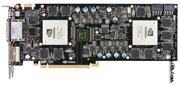
So that's two GF110 GPUs on a single graphics card connected through a NF200 bridge chip with a total of 1024 shader processors for both GPUs, and 3 GB of GDDR5 memory, all that on a 12-layer 11" PCB. the GPUs each get 10 power phases. Cooling wise NVIDIA extends the vapor-chamber cooling, yet now they make use of a dual-radiator design.
So yeah, it is hard to realize that the 9th of November last year these GPUs where released, this is how fast the product cycle is updated these days.
The new dual-GPU solution is of course DirectX 11 ready. With Windows 7 and Vista also being DX11 ready all we need are some games to take advantage of DirectCompute, multi-threading, hardware tessellation and new shader 5.0 extensions. DX11 is going to be good and, once tessellation kicks into games, better looking.
- GeForce GTX 590 : 1024 SP, 384-bit (2x), 365W TDP
- GeForce GTX 580 : 512 SP, 384-bit, 243W TDP
- GeForce GTX 480 : 480 SP, 384-bit, 250W TDP
- GeForce GTX 470 : 448 SP, 320-bit, 225W TDP
The GPU that empowers it all has small architectural changes compared to the initial GTX 480 FERMI design (which GF110 is based on), some stuff was stripped away and some additional functional units for tessellation, shading and texturing have been added. Make note that the GPU is still big, as the fabrication node is still 40nm. TSMC canceled the 32nm fab node preventing this chip from being smaller.
The two GF110 graphics processors have sixteen shader clusters embedded in them (called SMs) bringing a full 512 shader processors per GPU.
To keep TDP, power consumption and noise levels at really acceptable values, NVIDIA did keep the clock frequency and thus voltage lower than the GTX 580. That's 607 MHz on the graphics processors and 3414 MHz (effective data-rate) on the GDDR5 memory. But that will still chunk out ridiculous performance numbers of course.
| GeForce 9800 GTX |
GeForce GTX 285 |
GeForce GTX 295 |
GeForce GTX 480 |
GeForce GTX 580 |
GeForce GTX 590 | |
| Stream (Shader) Processors | 128 | 240 | 240 x2 | 480 | 512 | 1024 |
| Core Clock (MHz) | 675 | 648 | 576 | 700 | 772 | 607 |
| Shader Clock (MHz) | 1675 | 1476 | 1242 | 1400 | 1544 | 1215 |
| Memory Clock (effective MHz) | 2200 | 2400 | 2000 | 3700 | 4000 | 3414 |
| Memory amount | 512 MB | 1024 MB | 1792 MB | 1536 | 1536 | 3072 |
| Memory Interface | 256-bit | 512-bit | 448-bit x2 | 384-bit | 384-bit | 384-bit |
| Memory Type | gDDR2 | gDDR3 | gDDR3 | gDDR5 | gDDR5 | gDDR5 |
| HDCP | Yes | Yes | Yes | Yes | Yes | Yes |
| Two Dual link DVI | Yes | Yes | Yes | Yes | Yes | Yes |
| HDMI | No | No | No | Yes | Yes | Yes |
Memory wise NVIDIA has sizable and expensive memory volumes due to their architecture, we pass 1 GB per GPU as standard these days for most of NVIDIA's series 500 graphics cards. Each memory partition utilizes one memory controller on the respective GPU, which will get 256MB of memory tied to it.
- The GTX 590 has six (x2) memory controllers (12x256MB) = 3072 MB of GDDR5 memory
- The GTX 580 has six memory controllers (6x256MB) = 1536 MB of GDDR5 memory
As you can understand, the memory partitions, bus-width and combination of GDDR5 memory (quad data rate) allow the GPU to work with a high framebuffer bandwidth (effective). Let's put most of the data in a chart to get an idea and overview of some specific changes:
| Graphics card | GeForce GTX 470 | GeForce GTX 480 | GeForce GTX 580 | GeForce GTX 590 |
| Fabrication node | 40nm | 40nm | 40nm | 40nm |
| Shader processors | 448 | 480 | 512 | 1024 |
| Streaming Multiprocessors (SM) | 14 | 15 | 16 | 32 |
| Texture Units | 56 | 60 | 64 | 128 |
| ROP units | 40 | 48 | 48 | 96 |
| Graphics Clock (Core) | 607 MHz | 700 MHz | 772 MHz | 607 MHz |
| Shader Processor Clock | 1215 MHz | 1401 MHz | 1544 MHz | 1215 MHz |
| Memory Clock / Data rate MHz | 837 / 3348 | 924 / 3696 | 1000 / 4000 | 854 / 3414 |
| Graphics memory | 1280 MB | 1536 MB | 1536 MB | 3072 MB |
| Memory interface | 320-bit | 384-bit | 384-bit | 384-bit |
| Memory bandwidth | 134 GB/s | 177 GB/s | 192 GB/s | 164 GB/s per GPU |
| Power connectors | 2x6-pin PEG | 1x6-pin PEG, 1x8-pin PEG | 1x6-pin PEG, 1x8-pin PEG | 2x8-pin PEG |
| Max board power (TDP) | 215 Watts | 250 Watts | 244 Watts | 365 Watts |
| Recommended Power supply | 550 Watts | 600 Watts | 600 Watts | 700 Watts |
| GPU Thermal Threshold | 105 degrees C | 105 degrees C | 97 degrees C | 97 degrees C |
So we talked about the core clocks, specifications and memory partitions. Obviously there's a lot more to talk through. Now, at the end of the pipeline we run into the ROP (Raster Operation) engine and each GF110 GPU has 48 units for features like pixel blending and AA. There's a total of 64 texture filtering units per GPU available for the GeForce GTX 590. The math is simple here, each SM has four texture units tied to it.
- GeForce GTX 590 has 2 x (16 SMs X 4 Texture units) = 64 x 2 = 128 TUs
- GeForce GTX 580 has 16 SMs X 4 Texture units = 64 TUs
Though still a 40nm based chip, the GF110 GPU comes with almost 3 billion transistors embedded into it. So that's 6 billion transistors active in your PC -- if the Sims still doesn't run smooth... I dunno what would do the job ;)
The TDP is roughly 365 Watts, a very respectable number really. TDP = Thermal Design Power. Roughly translated, when you stress everything on the graphics card 100%, your maximum power consumption is the TDP.
The GeForce GTX 590 comes with two 8-pin power connectors to get enough current and still have some for overclocking.