A meet and greet with the GTX 295 Single PCB
A meet and greet with the GTX 295 Single PCB
On the next few pages we'll show you some photos. The images were taken at high-resolution and then cropped and scaled down. The camera used was a Canon 450D 12 MegaPixel.

Right then, so as always... we show the packaging. Point of View's latest goblin is showing clearly on the packaging. What is that... a Merlin looking Gnome or something? hehe :)
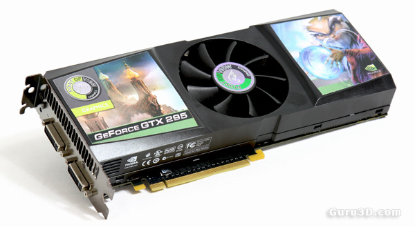
Unpacked, here we can spot the all new single PCB GeForce GTX 295. As explained over the previous pages... not one specification is different compared to the older model. All clock frequencies and features remain the same. To each outer side on the PCB we can find a GPU, and sitting in the middle a big fan.
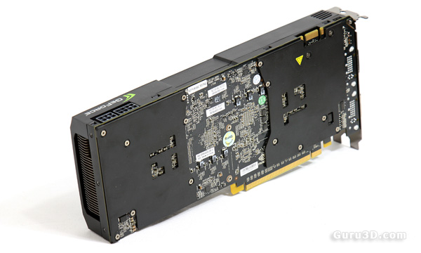
What I like about the new single PCB version is that the backside now has a back plate. The older model did not have this. In fact eVGA is even selling these separately as there is demand for it. The back plate of course offers a little more protection. Also spot to the upper right the SLI finger. Yes, you can go quad-SLI with this card. You can also mix and match the old dual-PCB version with this new single PCB based card. This is not a problem and the SLI fingers are positioned at the exact same spot.
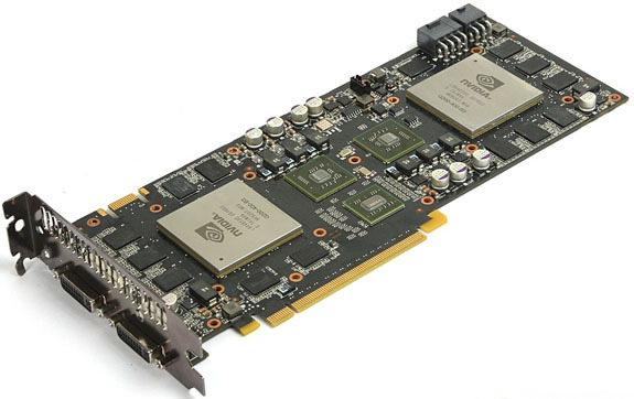
When we strip away the cooling, we get a much better insight of what is going on under the hood. Man, these GPUs are still looking colossal. Let's flip over the PCB and have a closer look.
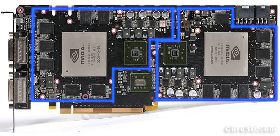
So if you look a little more closely, you'll notice that there are two graphics cards located on the PCB, each blue colored segment is a cluster of components. if you look at the middle and spot the three green chips, the lower one outside the blue boundaries is actually a switch chip responsible for the communication in-between the two GPUs. Each GPU is surrounded with memory chips (located at the backside as well). This PCB is surprisingly clean component wise. What a fascinating sight, isn't it? And yes I know I know... I'm being totally geeky right now :)
