Product Innards
Product Innards
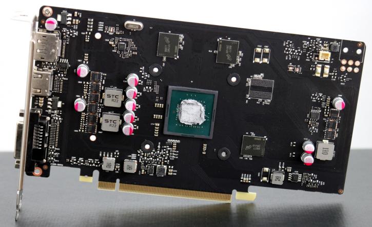
Alright, the good stuff, the nitty-gritty. With the main cooler is removed, you can see an all-black PCB and its components that make up for the products that are called GTX 1050 3GB edition. If you look at the memory placement throughout the PCBN, you can see one spot is left empty, yes the SMT traces reveal an empty GDDR5 memory location. This PCB was clearly designed for 4GB memory alright and simply might be the GeForce GTX 1050 Ti 4GB PCB being reused.
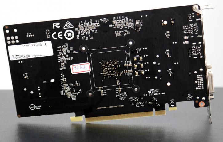
The backside of the card as well reveals a very simple and elegant design. Considering this is an early sample I blocked the serials and SKU code. But let's zoom in a bit at all the primary components.
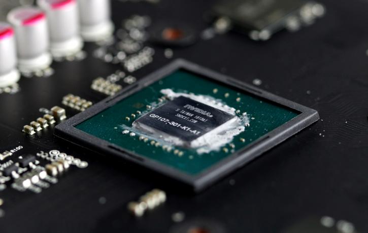
Here we have the GPU. Now, if it was a regular GeForce GTX 1050, you would see a GP107-300 GPU here. This indeed is a new SKU tagged as GP107-301-K1-A1 and keep in mind, the GP107-400-A1 graphics processor would be a GTX 1050 Ti is featuring 768 shader cores. So it is an official SKU for the GTX 1050 3GB. The GPU die is made from with a 14nm fab process with a transistor count of 3.3 billion and a die size of 132 mm². Little more needs to be said about it.
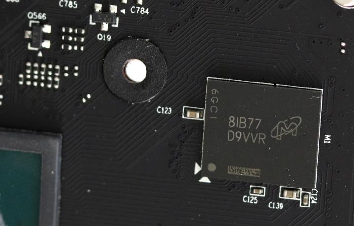
GDDR5 memory chips are made by Micron. The GDDR5 chips from Micron, are a really familiar series, SKU code D9VVR is actually rated at 2000 MHz (=8000 MHz GDDR5 effective data-rate) but has been configured for 7 Gbps. We'll demonstrate how far we can tweak it in the overclocking segment of this article. Creating some memory bandwidth greatly helps this card with some additional as the 1050 3B certainly is memory bandwidth deprived on that narrower 96-bit bus
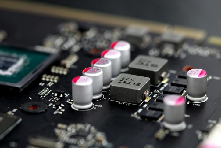
Dual power phases for the GPU and one (located to the right of the PCB) for the memory subsystem.
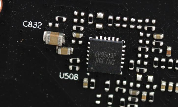
The uPI based uP9509P is a recent model voltage controller for NVIDIA cards, used quite a lot on ... yes, the GeForce 1050 Ti.
