The GF106 GPU
The GF106 GPU
Based on Fermi architecture, the 3rd chip derived from the Fermi family of GPUs is now born. The GeForce GTS 450 series is to be based on a new chip. Initially the Fermi architecture that you have all seen on the GTX 465, 470 and 480 is based on the GF100 chip. Then the upper mid-range and very successful GeForce GTX 460 was based on the GF104, a smaller chip with less transistors (2.1 Billion to be precise), called the GF104.
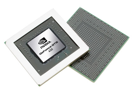 The GeForce GTS 450 is based on the GF106, this is a less complicated chip to manufacture with smaller transistor count directly relates to better yields, better heat levels, better voltages and thus a better TDP as well. The GF106 has a transistor count of 1.17 billion, based on a 40nm fabrication process.
In the initial release this GF106 GPU will be used solely for one SKU, a GeForce GTX 460 with 768MB of graphics memory and the GeForce GTS 450 that is armed with 1024MB of memory. That memory is quad data-rate, gDDR5 memory that runs over a 128-bit wide bus.
The GeForce GTS 450 comes with 192 shader processors spread out over four Streaming Multi-processor clusters (SM). That translates into a Texture Memory Unit count of 32, and thus 16 ROPs.
The reference core clock frequency of this product is 783 MHz, the shader processors are clocked at a tact frequency of 1566 MHz, and the 128-bit gDDR5 memory has an effective data rate of 3600 MHz.
This package is intended to create a product that replaces the GeForce GTS 250 and will compete with the Radeon HD 5750 series.
The GeForce GTS 450 cards will be fully fledged DirectX 11 class cards with nice tessellation performance and the full DX11 API feature set. Though only a handful of games really show significant DX11 class quality, we really feel that if you are in the market for a new graphics card, DX11 is obviously the path to follow.
Let's compare some of the specs of the GeForce GTX 450, the GeForce GTX 460 and 465.
Reference specifications:
| Graphics card | GeForce GTS 450 | GeForce GTX 460 | GeForce GTX 465 |
| Graphics Processing Clusters | 1 | 2 | 3 |
| Streaming Multiprocessors | 4 | 7 | 11 |
| Shader processor | 192 | 336 | 352 |
| Texture Units | 32 | 56 | 44 |
| ROPs | 16 | 32 | 32 |
| Core Clock | 783 MHz | 675 MHz | 607 MHz |
| Shader Clock | 1566 MHz | 1350 MHz | 1215 MHz |
| Memory Data rate | 3608 MHz | 3600 MHz | 3200 MHz |
| Memory | 1024MB GDDR5 | 1024MB GDDR5 | 1024MB GDDR5 |
| Memory interface | 128-bit | 256-bit | 256-bit |
| Memory bandwidth | 57.7 GB/s | 115.2 GB/s | 102.6 GB/S |
| Texture Fillrate Bilinear | 25.1 GigaTexels/sec | 37.8 GigaTexels/sec | 26.7 GigaTexels/sec |
| Fab node | 40nm | 40nm | 40nm |
| TDP | 106 Watts | 160 Watts | 200 Watts |
So yes, compared to the GTX 460 the GTS 450 is quite... castrated. Now if we look closely at the engine, then you can see and calculate that the 192 Shader Processors based GF106 has in fact four Streaming Multi-Processor clusters partitions. Four 48 Stream Processor clusters are enabled = 192 Shader Processors. But we expect other SKUs in the future as well with one or more SMs disabled.
|
click to enlarge |
Here's the GPU block diagram setup, one graphics processing cluster tied to four SMs, each with 48 Shader Processors and two 64-bit memory controllers. The GF106 was allowed to keep its 256KB L2 cache memory.
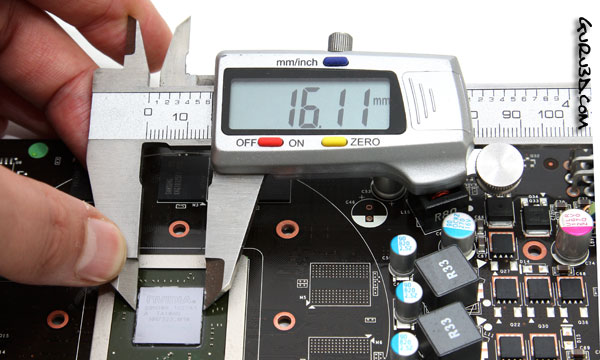
Die size wise NVIDIA these days absolutely refuses to give us numbers. So we measured it ourselves, the die is 16 by 16 mm (see photo below).
So the card in its baseline/reference setup will be clocked at 783 MHz on the core frequency, and in NVIDIA's typical 1:2 setup mode 1566 MHz on the shader processors. There will be good overclocking headroom left on these boards, 850 MHz should not be an issue, even without voltage tweaking.
The gDDR5 memory will be clocked at a shy 3.6 Gbps which is 3608MHz effectively (902 MHz (x4) quad data rate). As such, the GPU has two 64-bit memory controllers tied to it which boils down to 128-bit memory.
The GeForce GTS 450 cards are based on a dual-slot cooling design and come with two dual-link DVI and a mini-HDMI connector. HDMI will pass sound through, including bit streaming support for Dolby TrueHD and DTS-HD Master Audio.
Being a mid-range product, only 2-way SLI will be allowed and thus you'll only see a single SLI finger/connector on the PCBs. Okay, the next stop will be an extensive photo-shoot of the product(s) tested today.