The Broadwell-H architecture
The Broadwell Architecture
We'll address some key aspects and a technical overview of the technology and architecture first. Chances are good that you already have learned about this information over time. Right lets step back a few generations and start at Sandy Bridge at 32nm. Sandy Bridge really was a completely new architecture, its successor Ivy Bridge did share a lot of common denominators. When we look at Sandy versus Ivy Bridge, the foremost complicating factor was moving the architecture towards a smaller production node; Ivy Bridge is a 22 nm processor series. Haswell then, is a 22 nm product yet based on a FinFET process that uses a non-planar transistor that sits around the gate on three sides. Built using a 22 nm process, Haswell is the "tick" in Intel's "tick-tock" development cycle, so Ivy Bridge was just a process size shrink from Sandy Bridge's 32 nm to 22 nm.
We now land at Broadwell which is a Tick in the release schedule, soon to followed by a Tock, Skylake. For Broadwell several things changed, an increasingly powerful graphics engine and that fabrication shrink at the 14nm nod, this allows for an even more power friendly processor. The 5th generation processors there will of course be a distinction per processor segment (i3/i5/i7). What you get in terms of features and what you need to remember limitation wise:
- Desktop Core i7 processors have four cores / eight hyper-threads / Up to 6 MB L3 cache
- Desktop Core i5 processors have four cores / NO hyper-threading / Up to 4 MB L3 cache
- Desktop Core i3 processors have two cores (these are unannounced)
| Microarchitecture | CPU series | Tick or Tock | Fab node | Year Released |
|---|---|---|---|---|
| Presler/Cedar Mill | Pentium 4 / D | Tick | 65 nm | 2006 |
| Conroe/Merom | Core 2 Duo/Quad | Tock | 65 nm | 2006 |
| Penryn | Core 2 Duo/Quad | Tick | 45 nm | 2007 |
| Nehalem | Core i | Tock | 45 nm | 2008 |
| Westmere | Core i | Tick | 32 nm | 2010 |
| Sandy Bridge | Core i 2xxx | Tock | 32 nm | 2011 |
| Ivy Bridge | Core i 3xxx | Tick | 22 nm | 2012 |
| Haswell | Core i 4xxx | Tock | 22 nm | 2013 |
| Broadwell | Core i 5xxx | Tick | 14 nm | 2014 & 2015 for desktops |
| Skylake | Core i 6xxx | Tock | 14 nm | 2015 |
| Kabylake |
Core i 7xxx |
Tock | 14 nm | 2016 |
| Cannonlake | Core i 8xxx? | Tick | 10 nm | 2017 |
With Skylake so close to launch, the Broadwell for desktop series feel a little off, timed a bit wrong. The most prominent feature for this processor however is its improved GPU, if an IGP however is not what you are after, seriously my fellow Gurus, wait for Skylake please. But hey, 14nm is here. let's have a look.
Core Core i7-5775C and i7-5775C
Today we test the Core i7-5775C, it is a new quad-core processor based on the afore mentioned Broadwell architecture and supersedes the Core i7-4770 / 4790 processor range (in design). Two desktop Broadwell processors have been released though, the Core i7 5775C selling at just over 400 EURO and Core i5 5675C priced at just over 300 EURO (this latter model does not have hyper-threading).
The Core i7-5775C comes with a base clock frequency of 3.3 GHz and a maximum Turbo allowance towards 3.7 GHz. This chip has hyper-threading and your OS will see it as an 8-core products. The CPU has 1 MB L2 cache (256 kB per physical core). Then there is a 6MB shared L3 cache. The integrated memory controller remains dual-channel, officially supporting up-to 1600 MHz, but we all know how high these puppies can clock. The TDP for this processor is lower opposed to Haswell, 65 Watt.
The Core i5 5675C is fairly similar product, yet clocked a notch slower at a 3.1 GHz base clock and 3.6 Turbo allowance. This processor as stated does not have hyper-threading. Also it has slightly less L3 cache at its disposal, 4 MB.
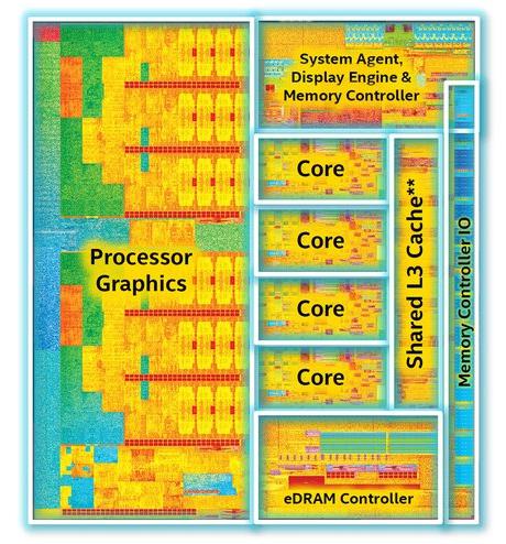 Broadwell-H block diagram |
|||||
| i7-5775C | i7-5775R | i5-5675C | i5-5675R | i5-5575R | |
| Base Frequency | 3.3GHz | 3.3GHz | 3.1GHz | 3.1GHz | 2.8GHz |
| Turbo Frequency | 3.7GHz | 3.8GHz | 3.6GHz | 3.6GHz | 3.3GHz |
| Cores | 4 | 4 | 4 | 4 | 4 |
| Threads | 8 | 8 | 4 | 4 | 4 |
| Graphics | Iris Pro 6200 | Iris Pro 6200 | Iris Pro 6200 | Iris Pro 6200 | Iris Pro 6200 |
| EUs | 48 | 48 | 48 | 48 | 48 |
| Graphics Frequency | 1150MHz | 1150MHz | 1100MHz | 1100MHz | 1050MHz |
| DRAM Frequency | 1600MHz | 1600MHz | 1600MHz | 1600MHz | 1600MHz |
| L3 Cache | 6MB | 6MB | 4MB | 4MB | 4MB |
| L4 Cache (eDRAM) | 128MB | 128MB | 128MB | 128MB | 128MB |
| Package slot | LGA | BGA | LGA | BGA | BGA |
| Price | $366 | $348 | $276 | $265 | $244 |
The Broadwell cache memory consists of a 32 KB L1 Data cache, 32 KB Instruction cache (= 64 KB L1) and then we spot a 256 KB L2 cache per core.
Then there's a L3 cache that is shared in-between the CPU cores which is 6 MB in total for the Core i7 processors and 4 MB for the Core i5 series. The L3 cache is where the magic happens, surrounded by the segments inside the die, the L3 cache sits in the physical form of a ringbus. Thus the L3 cache can be used by the processor cores and also the graphics core. Compared to the 4770/4790 processors that you guys mostly have, this is not a significant speed increase. Actually processor performance wise you can expect a fairly similar performing product. There is however one big change, and that is the integrated graphics processor. You can house the new processors on motherboards with the H97/Z97Chipset. For end consumers like you and me the H97 chipset is less performance targeted and comes with better support for HTPC monitor connectivity. The Z97 chipset is targeted at performance and enthusiast end users allowing much more tweaking and providing performance features. It also brings SATA Express and PCIe M.2 SSD connectivity to the platform. Please do make sure you have the latest motherboard firmware installed to be able to get full support. Some Z87 and H87 might work as well, but these will definitely need a compatible Firmware update before seating and using the processor.
