3
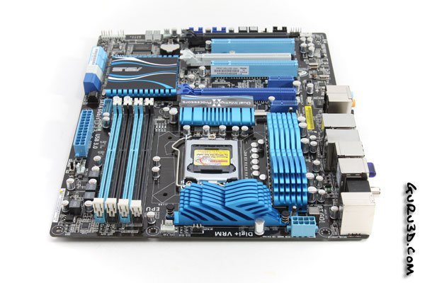
When we flip the board around 90 degrees we stumble into the processor socket, LGA1155, a new socket required for the upcoming Sandy Bridge processors. Here we can also see a 8-pin CPU power header conveniently placed at the far side of the edge. The VRM/MOSFET/Choke area is nicely covered with passive cooling.
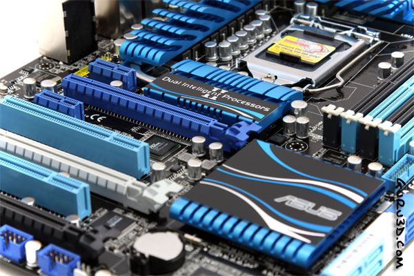
If we zoom in a little we can spot lots of room around socket LGA 1155, also we spot quality capacitors and solid core chokes. The component selection was done properly alright.
Key feature of this board is its Dual Intelligent Processors 2- with DIGI+ VRM. DIGI+ VRM combines digital and analog VRM design, delivering less switching delay while offering better accuracy at the same time. Delivering better permeability and less power loss, meaning less heat will be produced under the compared with the traditional digital VRM design.
With control options available under both the BIOS and windows, allowing the users with the complete control over the power solution. All the way in the middle we see a PLX ExpressLane PEX 8608 8-lane PCI Express switch IC by the way.
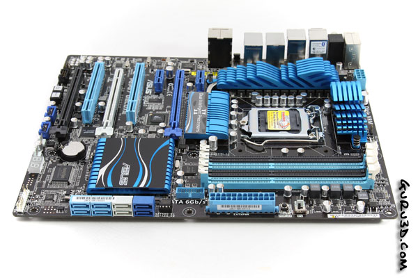
The ATX motherboard power connector is position properly, with above it the DDR3 DIMM slots. the motherboard can take up-to 16GB of memory clocked at 1333 MHz. Overclocked BIOS options allow for settings at 1600/1866 and even 2133 MHz as well, the manual even mentioned 2400 MHz, yet overclocked.
